TQFP is a type of Integrated Circuit (IC) package with a smaller footprint. Over the years, it has become a favorite for applications in the military and defense markets. In this blog post, you will find out what it means and the clear differences between TQFP and LQFP.
Understanding what a QFP Means
TQFP is an IC package under QFP, which stands for Quad Flat Package. It is a type of Integrated Circuit (IC) package family that uses gull wings that extend from the four sides of the package.
How Does a Thin Quad Flat Package (TQFP) Work?
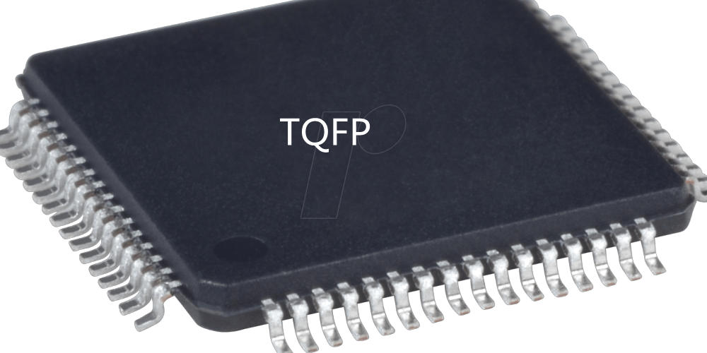
The full name is Thin Quad Flat Package. As the name suggests, it is a thin variant of the IC packages under QFP. For emphasis, it is one of the thinnest and has the following compositions:
- Led pitch range from 0.48 to 0.8mm
- Varied body sizes, ranging from 7×7, 14×14, and 10×10.
- Increased lead or pin count, starting from 32 up to 256 pins.
- Up to 1.4mm of body thickness.
Packaging Process
The process of packaging the TQFP IC involve using a well-controlled, low loop wire bonding process and package control. These are utilized during the molding process.
The Role of Flat Packaging in TQFP
Flatpack package is a type of Integrated Circuit (IC) packaging process used in the TQFP. At the time the Quad Flat Package (QFP) became popular, Europe was the major market using it. The QFP would later become popular in the United States in the early nineties.
The flatpack package is now a United States’ military standard for packaging surface mount component-based components into a Printed Circuit Board (PCB).
Tackling Industry Problems with Thin Quad Flat IC Package
TQFP also tackles or solves some of the industry problems, as they pertain to circuit board designs. The following are some of the problems the package solves:
1. IC Package Portability
Not all Integrated Circuit (IC) packages are portable. Using TQFP assures of getting the much-needed portability, as it is best described as a thin end-product profile.
2. Die Shrinking
TQFP solves the challenge of the die shrinking of becoming practically unnoticeable below the package or wherever it is placed.
Preventing die shrinking on the package is enabled via the increased thickness of the die wire up to 11mils (280um) range.
TQFP Gains Mainstream Adoption Faster
Designing a circuit board with a market in mind helps to facilitate the adoption or purchase as soon as it is released.
TQFP is primarily used in making circuit boards for specific markets. The primary markets are those cost-sensitive applications that require the highest levels of weight and thickness.
The following are examples of some of the supported applications:
- Chipsets for Personal Computers (PCs)
- ASICs
- Multimedia devices
- DSP Slices
- Microcontrollers (MCUs)
- Gate Arrays
- Microprocessors
- Logic Integrated Circuits (ICs)
Comparing TQFP to SOIC
Both Thin Quad Flat Package (TQFP) and Small Outline Integrated Circuit (SOIC) package are types of IC packages.
Both are similar in the sense that they use the same type of lead – the gull-wing shaped lead. However, they have one clear difference. The difference between the two is that while the TQFP uses the gull-wing shaped lead on the four (4) sides of the package, the SOIC only uses it on two of the package’s sides.
Thus, SOIC is a dual-sided IC package, while TQFP is a quad-sided Integrated Circuit package.
TQFP vs. LQFP: The Major Difference

Thin Quad Flat Package (TQFP) is often compared to the Low-profile Quad Flat Package (LQFP) because they both belong to the broader Quad Flat Package (QFP).
The major difference between the two lies on the height. While the TQFP has a height less than 1.2mm. the LQFP’s height is up to 1.7mm.
Advantages of the TQFP IC Package
If you are looking for reasons to use the TQFP IC package, we have lots of them. Here are some of the benefits of choosing the package:
Green Materials
By “green materials,” we mean that the materials used in making the TQFP package are lead-free and low alpha. These materials are also RoHS compliant and standardized.
Limitations to Working with the TQFP IC Package
Expect some of the following design lapses or challenges when using a TQFP on a circuit board project:
1. Decreased Spacing
As the thinnest IC package under QFP, TQFP has limited spacing. The limited spacing option is because of the drastic reduction of available spaces from 50mil down to 20mil and then 12mil.
The decreased spacing was done to provide more rooms to add more pins into the package.
2. Challenges with Solder Bridges
Decreasing the spaces to add more pins seemed a great idea, but it has led to placing more demands or pressures on the soldering process.
Solder bridges are now more likely when working on the TQFP IC package.
How TQFP Combines Limited Spacing with Improved Pin Counts
Thin Quad Flat Package may have limited spacing but it makes up for that by integrating more pins.
What’s more? It can integrate specific gate arrays, such as the Ball Grid Array (BGA) and the Pin Grid Array (PGA) IC packages.
Making that integration helps not to only reduce the challenges associated with spacing the leads. It also helps to enable connections around the package and to increase the pin count of other smaller IC package sizes.
Benefits of TQFP’s Surface Mount Technology (SMT)
Surface Mount Technology (SMT) is one of the packaging types/processes for Integrated Circuits (ICs).
It offers the following benefits to the TQFP:
Automated Methods
SMT typically uses automated processes to place the components on the circuit board. The automation also helps to reduce human interference, thereby, saving costs.
Better EMC Performance
Electromagnetic Compatibility or EMC is the ability of multiple components and electronic devices to work perfectly even though they are in proximity to the other.
TQFP matches that description because of the enhanced EMC performance exclusive to the Surface Mount Technology (SMT).
Conclusion
TQFP is the thinnest of the IC packages under Quad Flat Package (QFP). The errors during the design can be fixed in real-time, thanks to the molten solders pulling the components together in the Printed Circuit Board (PCB).