Today’s or the modern-day’s consumer electronics is taking a different shape, especially with the introduction of newer process technologies. The process of optimizing circuit boards has evolved greatly with transistors taking the lead.
However, it is imperative to protect not just the transistors, but also prevent the internal components from getting overly exposed to contaminants. That is one of the major reasons why you need to invest in the TO-92 package.
In this article, you will discover some of the best attributes of working with this package.
What is the TO-92 Package?
It is a type of semiconductor packaging for transistors, especially those manufactured or processed with the Through-Hole Technology (THT).
Also known as the Transistor Outline, Case Style 92, the TO-92 package helps to protect the transistors, while maximizing the compact real estate in the Printed Circuit Board (PCB).
Typical Applications
TO-92 is typically used for low-power applications, particularly the linear regulators, MOSFETs and Through-Hole transistors.
TO-92’s use cases date back several decades ago, sometime in 1966 when Motorola used the package for the 2N3904 devices.
Configuration of the TO-92 Package
Here are some of the properties of the package and how they stand out:
1. Thermal Dissipation
Dissipating or channeling heat out of the semiconductor package to the Printed Circuit Board (PCB) is easier, with the plastic and epoxy materials the TO-92 is typically made of.
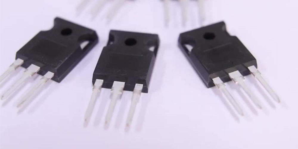
2. Protruding Leads
TO-92 uses three (3) leads and these protrude from the bottom of the semiconductor package. It also using the three (3) leads, because that is one of the major expectations of a package looking to be used in transistor packaging.
3. Lead Spacing
The space between the leads is typically 0.5-inch or 1.27mm. These leads are also bended in a way that there is enough room or space for additional wiring on the package. The typical spacing made here is 0.10-inch or 2.54mm.
We also like to point out that the configuration of the leads is in line with the three-phased design of the package, which cut across the Emitter, Base and Collector.
Although the above is the primary configuration, it is tenable with the JEDEC or 2N transistors. Therefore, depending on the TO-92 manufacturer, it may be possible to alter the arrangements of the configurations.
Orientation of the TO-92 Package
The package is optimized in a way that the back is semi-circularly-shaped while the face is flat. The flat face (surface) typically comprises numbers printed with a machine. These numbers denote the specific part number of the TO-92 transistor package.
Identifying the TO-92 Semiconductor Package
Note that the package is typically made by both Pro Electron and Japanese manufacturers. Thus, the specific numbering or part identification systems are in place to know the actual manufacturer or the origination of the package.
For example, TO-92 packages made by Pro Electron typically start with the BC part number, though SC is also possible.
TO-92 packages manufactured by Japanese companies tend to have the 2N part number at the beginning.
However, there may be a disparity on the manufacturer when the TO-92 package only has an alphabet followed by a few numbers.
Technical Properties of the TO-92
Below are some of the properties of the package:
1. Varied Thermal Resistances
The heat, power or thermal resistances of the TO-92 package varies by the components. For example, the plated through-holes TO-92 has a 0.2-inch-square thermal resistance pad, per lead. On the other hand, the package-only TO-92 has a thermal resistance of 220-degree Celsius/W, while that of the plated through-holes-only TO-92 is 175-degree Celsius/W.
2. Process Technology
TO-92 is a 3-lead transistor package manufactured with the Through-Hole Technology (THT).
3. Typical Usages
The common applications or usages of the TO-92 include digital 1-wire temperature sensors, linear regulators and active linear analogue temperature sensors.
The package also has Three-Dimensional (3D) models, namely: MOSFETs and BJTs.
Generally, the TO-92 transistor package is ideal for the low-power or low-current through-hole transistors.
It also covers other forms or variants of voltages, including the high-voltage and high-current transistor applications.
4. Board-Specific Configurations
Some Printed Circuit Boards (PCBs) appear to have been modelled to work with the basic configurations of the Transistor Outline (TO) packages.
That changes with the TO-92 package, which offers a circuit board-specific configuration. Depending on the application or usage, circuit board units with pre-bent leads of the TO-92 package could be optimized for the specific layouts of the Printed Circuit Boards (PCBs).
Benefits of the TO-92 Transistor Package

If you are looking for reasons to work with the TO-92, here are some of its advantages:
Compact Size
Since it doesn’t take much circuit board space, TO-92 is arguably one of the compact-sized transistor packages you can work with.
Affordability
Depending on the TO-92 manufacturer, the package can be made readily available and in large quantities.
Wide Usage
TO-92 is ideal for low-current or low-power applications, but that is just the starting point. The transistor package has since been used to optimized circuit boards with higher currents and voltages.
Due to the wide applications, transistor consumers tend to use it to offer varied uses ranging from circuit board prototyping and beginner’s learning classes.
TO-92 has Several Variants
You can find several variations of the TO-92, ranging from the standard variant (TO-92) and the semi-standard variant labelled as TO-92/18.
Downsides to the TO-92 Transistor Package
Just as it has impressive benefits, the TO-92 transistor package also has a couple of downsides. These are some of the disadvantages of using the package:
Zero Pinout Standard
Unlike some of the popular transistor packages, the TO-92 doesn’t have a standard pinout. Thus, you may be unable to use it for pin or lead-specific applications.
TO-92 is not Ideal for High-Power Applications
Since the primary optimization is for low-power through-hole transistors, the TO-92 may not be ideal for the applications or devices requiring higher currents.
It Doesn’t have a Heatsink
The heatsink helps move thermal energy or (excessive) power from the transistor package to the circuit board.
TO-92’s package doesn’t have a heatsink, thus, making it impossible to do that. The compact size also makes it difficult to integrate a heatsink that could have helped in dissipating much heat.
To that end, you want to stick to the basic thermal dissipation capabilities, because going overboard might cause it to burn out quickly.
Final Words
The best method of using the TO-92 transistor package is to stick to using it with devices requiring low-power and which also don’t dissipate much heat at once. That way, the package lasts longer and fulfills the primary functions.