Flyback converter secondary output rectifier diodes or synchronous MOSFETs, placed on the high side (output power side) or on the low side (output ground side), the two cases, the power system EMI results will have a large difference. Usually, it is placed on the high end EMI effect is better, the margin is greater, the following analysis of the reason for this.
Switching power supply, the power device high-frequency turn-on, turn-off operation resulting in rapid changes in current and voltage is the main reason for EMI.
The inductance of the circuit and the rapid current changes in the parasitic inductance generate a magnetic field, which results in higher voltage spikes.
VL = LS – diL /dt
The capacitance of the circuit and the fast voltage changes in the parasitic capacitance produce an electric field, which results in higher current spikes: iC = C – duc /dt
iC = C – duc /dt
Magnetic and electric field interference noise, and the changing voltage and current and coupling channels such as parasitic inductance and capacitance are directly related to the main methods of controlling EMI are.
1, reduce the rate of change of voltage du / dt and current rate of change di / dt
such as control the switching speed of the switching tube, the external use of absorption circuits.

2, reduce the corresponding parasitic stray inductance and parasitic coupling capacitance
Such as the circuit where the switching tube is located as short as possible and use a wide PCB copper foil, reduce the voltage dynamic changes in the PCB copper foil area of the switching node; optimize the transformer structure, reduce the number of winding layers, the primary sandwich winding method, the primary and secondary winding between the increase in shielding copper or shielding winding.
3, the interference noise current compensation offset
Increase the compensation winding between primary and secondary windings, optimize the position of dynamic and static points of primary and secondary, so that the current signal of interference can cancel each other out. The node where the voltage does not change is called the static point; the node where the voltage changes is called the dynamic point.
Secondary output rectifier secondary or synchronous MOSFETs, placed on the high end and placed on the low side of the difference between EMI, is the third case above.
Flyback converter transformer secondary winding of the upper end and the switch node SW (power MOSFET drain) for the same name, as shown in Figure 1. C1 for the switch node SW and the lower end of the secondary winding between the parasitic capacitance; C2 for the positive end of the primary power supply and the upper end of the secondary winding between the parasitic capacitance; CSW for the switch node space parasitic capacitance; C3 for the output ground space parasitic capacitance.
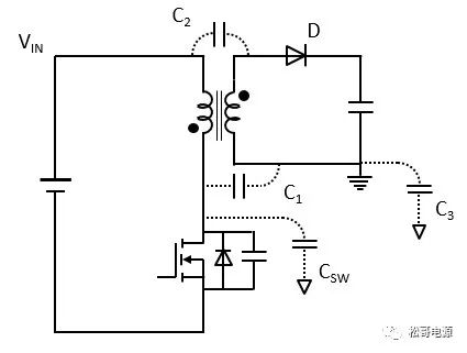
Figure 1 Parasitic capacitance of flyback converter
1, the output rectifier diode on the high end
The output rectifier diode is placed at the high end, the positive end of the input power supply and the lower end of the secondary winding (output ground) are the static points.
When the switching tube is turned off, the VDS voltage of the power MOSFET rises with a very large dV/dt, as shown in Figure 2.

Figure 2 Operating waveform of flyback converter
Under the influence of the primary and secondary parasitic capacitor C1 at dV/dt, the interference current signal I1 is generated between the primary and secondary. similarly, the voltage on the secondary winding rises at a certain dV/dt, and the interference current signal I2 is generated between the primary and secondary under the influence of the primary and secondary parasitic capacitor C2 at dV/dt. the currents I1 of C1 and I2 of C2, their directions are shown in Figure 3.
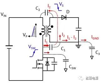
Figure 3 rectifier tube to put the high end of the current direction of parasitic capacitance
Interference current signals of the transformer secondary are to flow back to the detection equipment earth through the output ground space capacitor C3, therefore, the current IGND flowing through C3 is
IGND = I1 – I2
It can be seen that part of the interference current I1 flows through I2 to the primary, reducing the total interference current IGND, which is equivalent to compensation through C2, offset part of the interference current generated by C1.
2, the output rectifier diode at the low end
The output rectifier diode is placed at the low end, the positive end of the input power supply, the upper end of the secondary winding (power supply output) is the static point.
When the switching tube off, there is no interference current flowing in C2. The voltage at the lower end of the secondary winding, however, drops by a certain dV/dt, so that the total dV/dt between the parasitic capacitor C1 becomes larger, then the interference current signal I1′ is generated between the primary and secondary is greater than I1; at the same time, this current all flows to the space capacitor C3 at the output ground:.
IGND’ = I1′ > I1 > IGND
The currents I1′ of C1 and I3′ of C3, their directions are shown in Figure 4. It can be seen that the interference current generated by C1 can not be compensated by C2, offset, therefore, the EMI results become worse.

Figure 4 Current direction of rectifier tube discharge low side parasitic capacitor