I. Overview of SD card
1、Definition
SD card (Secure Digital Card), a new generation memory device based on semiconductor flash memory, is widely used in portable devices, such as digital cameras, personal digital assistants (PDA in foreign language) and multimedia players, etc.
2、Capacity class

3、SD card block diagram
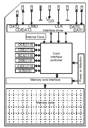
Pin Description.

4、The difference between SD card and TF card
TF card, also known as micro SD card, is 1/4 smaller than SD card and can be converted to SD card by “TF to SD card sleeve”.
II. Internal structure of SD card
(From SanDisk Secure Digital Card Product Manual Version 1.9)
1、 SD card internal structure sketch
The SD card is composed of SD card controller and memory array, and the communication interface between SD card and the outside world is SD Bus or SPI Bus.

2、 Storage array structure diagram
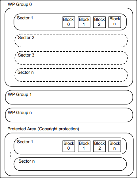
Block:
The unit (data transfer unit) in which reads and writes are performed, and its unit is “byte”.
Sector:
If CSD register ERASE_BLK_EN = 0, Sector is the smallest erase unit and its unit is “block”. the value of Sector is equal to the value of SECTOR_SIZE in CSD register + 1.
WP Group:
The smallest write protection unit, its unit is “sector”.
3、Buffer

The maximum capacity of Buffer of SD Card is defined in READ_BL_LEN and WRITE_BL_LEN of CSD register. their values are the same and it is possible to exceed 512 bytes, despite this Block should be set to 512 bytes because 512 bytes is the data boundary (this sentence is not too understandable). That is, there is a data transfer buffer Buffer on the SD card, which may be different for different products, but the Buffer should be set to 512 bytes when in use.
Reference.

The card buffer size is described as maximum block length in the Card Specif ic Data (CSD) register for memory cards (for cards compliant with the Physical Layer SpecificaTIon, READ_BL_LEN and WRITE_BL_LEN shall be the same) and in the Card InformaTIon Structure (CIS) for SDIO cards. Physical Layer SpecificaTIon re-defines that maximum block length is only used to calculate capacity of memory card. Even though it indi cates larger than 512 bytes, block length shall be set to 512 byte for data transfer. This is because 512 bytes block l ength is required to keep compaTIbility with 512 bytes data boundary.
(摘自《Simplified_SD_Host_Controller_Spec.pdf》)
4, “Storage Array Block” – the smallest storage unit
The information on the Block generally refers to the smallest unit of data transfer, the definition of this value is for data transfer, CRC checksum, etc..
Storage arrays usually use the structure of NandFlash, obviously can not be accessed by byte, and the “storage array Block” is discussed here refers to this concept. Unfortunately, at present, I have not found information to discuss this issue, so this section is the author’s own speculation.
According to my speculation, the storage array block should be 512Byes, because a lot of data are revolving around 512Bytes. For example, the smallest erase unit is 512Byes, the smallest read and write units should be set to 512Bytes, then it is reasonable to speculate that this value.
5, SD card special function registers
CID: width 128 bits, the card identification number
RCA: width 16 bits, the relative address of the card, determined at the time of initialization
CSD: width 128 bits, card description data: information about the card’s operating conditions
SCR: width 64 bits, SD card configuration register: SD card specific information data
OCR: width 32 bits, operation condition register
III. SDIO interface

Four, SD card protocol of data read, write, erase
1、SD card write data block
When executing the write data block command (CMD24-27), the host transfers one or more data blocks from the host to the card, while transmitting a CRC code at the end of each data block. The host transmits the data, the SD card receives the data and saves the data in Buffer. When the accumulated received data reaches the Block length, the SD card treats the next data as the CRC check code and starts the data checksum. If the CRC checksum is incorrect, the card indicates the error via the SDIO_D line, and the transmitted data is discarded instead of being written, and all subsequent (in multi-block write mode) transmitted data blocks are ignored.
If the host transmits part of the data and the accumulated data length is not aligned with the data block, when block misalignment is not allowed ( parameter WRITE_BLK_MISALIGN of the CSD is not set), the card will detect the block misalignment error before the first misaligned block ( set the ADDRESS_ERROR error bit in the status register). The write operation is also aborted when the host attempts to write a write-protected area, at which point the card sets the WP_VIOLATION bit.
The maximum length of the data block Block is defined in WRITE_BL_LEN in the CSD, but it should be set to 512 Byets with the CMD16 instruction during data transfer, not caring if WRITE_BL_LEN is 1024 or 2048 Bytes.
It is also important to note that the length of the Block is also set with reference to the WRITE_BL_PARTIAL of the CSD register; when WRITE_BL_PARTIAL is 0, then the Block can only be set to 512 Bytes; if WRITE_BL_PARTIAL=1, then the Block is allowed to be set to a smaller block If WRITE_BL_PARTIAL=1, then the Block is allowed to be set to a smaller block, say one byte. The protocol is so specified, but according to my analysis, if so the production of SD cards will be very complex (the unit of writing can be bytes), the price will also be very high. I tested my own SD card, WRITE_BL_PARTIAL is equal to 0, that is, does not support the “block part write” function.
2、SD card read data block
In the read data block mode, the basic unit of data transmission is the data block Block. to ensure the correct data transmission, the transmission of a data block Blcok after there is a CRC check code. The author believes that the host can treat the next data as a CRC check code and check it after receiving the Block length data cumulatively, the software.
The maximum value of Block is defined in the CSD (READ_BL_LEN), but it should be set to 512 Byets with the CMD16 instruction during data transmission, not caring whether READ_BL_LEN is 1024 or 2048 Bytes.
If the READ_BL_PARTIAL in the CSD register is equal to 1, the smaller data block that can be transferred, the smaller data block is the one where the start and end addresses are completely contained in one physical block. In fact, the protocol states that READ_BL_PARTIAL is always equal to 1, which means that on any SD card it is allowed to “read partial blocks”, the minimum bytes of the read block being 1 Bytes. The 128 bytes read must be within the 512 Bytes boundary, and cannot cross the boundary (in fact, because the storage array is in 512 Bytes, reading “partial blocks” can only be within a block, and is not allowed to read across blocks).
3、Erase SD card
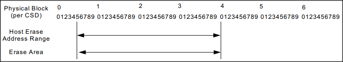
CSD register ERASE_BLK_EN determines the minimum erase unit of SD card.
When ERASE_BLK_EN is equal to 0, the smallest unit of host erase is sector. For example, a Sector contains 32 Blocks, and the start address is 5 when erasing, and the end address is 40, then the actual erased blocks are from 0 to 63.

When ERASE_BLK_EN is equal to 1, the minimum unit of host erasure is 512 Byetes. e.g. if the start address of the erase is 5 and the end address is 40, then the actual erased blocks are from 5 to 40.
V. SD card physical layer protocols
The protocol of SD card is relatively complex compared with the memory of SPI and I2C protocols, including the physical layer of SD card (mechanical package, pins, chip structure, command set, etc.), SD card interface (SDIO), SD host controller, and even the flow of software design, all of which are specified in detail.
1、Interface
① SDIO interface
参考《Simplified_SDIO_Card_Spec.pdf》

<1> CLK clock synchronization line
<2> CMD command signal line, the command issued by the master and the slave’s response to the command are transmitted through this line
<3> DAT[3:0] indicates the four data lines from which the data of the host and the slave are transmitted
② SPI interface

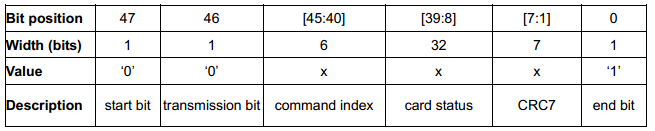
2、Command format

3、Response format
Take R1 as an example
4、The working status of SD card

5、Two kinds of SD card status information
① Card Status
The status information during the execution of the command, such as address misalignment error, block length error, card lock, ECC check error, etc.
blog.csdn.net/g_salamander
② SD Status
SD card’s proprietary feature, not often involved in programming. This status value has 512 bits and is not transmitted to the host through the command line, but through the data line.
Six, the STM32 and SD card with the peripheral – SDIO adapter
1, SDIO adapter structure diagram
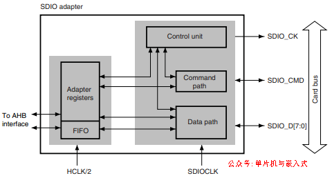
2、Command State Machine (CPSM)
The CPSM state machine is started when a command is sent and a response is received.
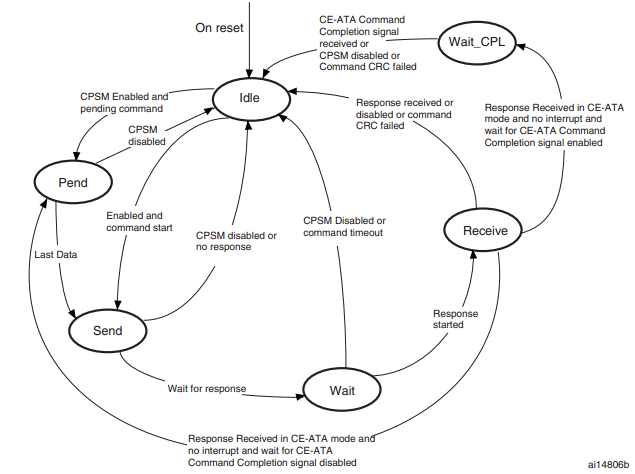
3、Data channel state machine
When data is transmitted, the data channel state machine is started.

4、FIFO
The data FIFO (first-in-first-out) subunit is a data buffer with send and receive units.
The FIFO contains a data buffer 32 bits wide per word, 32 words in total, and send and receive circuits. Because the data FIFO operates in the AHB clock region (HCLK/2), all signals connected to the SDIO clock region (SDIOCLK) are resynchronized. Depending on the TXACT and RXACT flags, the FIFO can be closed, enabled to transmit, or enabled to receive; TXACT and RXACT are set by the data channel subunit and are mutually exclusive.
When TXACT is active, the transmit FIFO represents the transmit circuit and data buffer
When RXACT is active, the receive FIFO represents the receive circuit and data buffer.
5、SDIO special function registers
SDIO power control register (SDIO_POWER)
SDIO clock control register (SDIO_CLKCR) : clock selection, frequency division
SDIO parameter register (SDIO_ARG)
SDIO command register (SDIO_CMD): control sending command
SDIO command response register (SDIO_RESPCMD): contains the command index in the response command
SDIO response 1..4 register (SDIO_RESPx): contains the card status information in the response command
SDIO data timer register (SDIO_DTIMER)
SDIO data length register (SDIO_DLEN): the length of read or write, usually is a multiple of 512
SDIO data control register (SDIO_DCTRL): control data read/write direction, enable transmission and other information
SDIO data counter register (SDIO_DCOUNT): When the DPSM state machine switches from Idle state to Wait_R or Wait_S state, the value of SDIO_LEN is loaded into this register.
SDIO status register (SDIO_STA)
SDIO clear interrupt register (SDIO_ICR)
SDIO interrupt mask register (SDIO_MASK)
SDIO FIFO counter register (SDIO_FIFOCNT): when DTEN in SDIO_DCTRL is enabled and DPSM is in Idle state, the value of SDIO_LEN/4 is loaded into this register
SDIO data FIFO register (SDIO_FIFO): read/write data buffer FIFO
Seven, SD card programming
SD card programming routines are available in the official STM32 firmware library, and the Wildfire development board has Chinese comments on the routines, so there is no need to post the source code into it. Here focus on the SD card programming process, mainly contains SD card initialization, SD card read, SD card write, SD card erase.
1、The content of SD card programming
SD card is mainly used to store data, so the core is to read and write. In order to achieve this goal, a responsive driver must be implemented.
The configuration process not only involves setting up the SD controller, but also setting the SD card to the appropriate state. When reading the state, not only the state of the SD controller is involved, but also the state of the SD card.
2、SD card initialization
① STM32 peripheral SDIO initialization
Port configuration, port clock, SDIO clock, DMA2 clock enable
SDIO register reset
Set the clock SDIO_CK below 400KHz, set the data line width, turn on the clock, turn on the SDIO power
② SD card power-on initialization
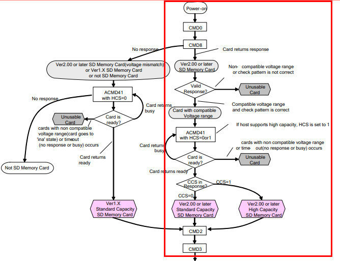
The power-on initialization process is shown in the above diagram. I think that the routine provided by the official library does not exactly follow the instructions of this flow chart. In fact, the official library routine only does the flow as shown in the red box in the above diagram, and nothing beyond that is covered.
The CMD0 command resets all cards.
The SD protocol states that the CMD8 command must be used before the ACMD41 is used during initialization. And the ACMD41 command is an application command, and the command CMD55 needs to be sent before it can be used.
The CMD8 command is to verify whether the power supply matches. the ACMD41 command constantly asks whether the SD card supports the voltage provided by the host, and asks whether the SD card is powered up and completed into the ready state. the ACMD41 command also asks the type of the SD card (SDSC, SDHC).
③ Card further verification, get card information
Send command CMD2 to get CID information.
Send command CMD3 to get RCA relative address. You can send CMD3 several times to get different RCA values, but only the last one is the valid RCA address.
Send the command CMD9 to get the CSD register.
④ Set SDIO to work in data transfer mode
Set the clock of SDIO to 24MHz and the width of data line to 4 bits.
Process the previously obtained CID and CSD into card information through SD_GetCardInfo function.
Select the card with matching address by CMD7 command, and deselect the other cards.
At this point, the initialization is completed.
3、Read a block of SD card
Clear the data control register (SDIO_DCTRL) to zero
Send command CMD16 to set the Block size of SD card
Call function SDIO_DataConfig to set SDIO data transfer method
Send command CMD17 to read a single block
Enable SDIO data transfer end interrupt
SDIO’s DMA transfer function enable
DMA setting, and enable
4、Write a block of SD card
Data control register (SDIO_DCTRL) is cleared to zero
Send the command CMD16 to set the Block size of SD card
Send command CMD24 to write a single block
Call function SDIO_DataConfig to set SDIO data transfer method
SDIO data transfer end interrupt enable
DMA setting, and enable
Enable the DMA transfer function of SDIO
Eight, SD card doubts
1, SD card after an erase, the content of which is 0, or 1?
The data at the card after an erase operation is either ‘0’ or ‘1’, depends on the card vendor. The SCR register bit DATA_STAT_AFTER_ERASE (bit 55) defines whether it is ‘0’ or ‘1’. (From “SD Specifications_Part_1_Physical_Layer_Specification_Ver3.00_Final_090416.pdf”)
That is, this is the chip manufacturer’s production process decision, you can learn through the SCR register DATA_STAT_AFTER_ERASE bit.
2, in the SDIO_DCTRL set the requirements of the transmission Block
The block size determines to what extent the host starts to send CRC checksum when sending data, and to what extent the SD card data is received and checked as CRC checksum when receiving data. block may also affect other timing. In the STM32’s SDIO register set, the bit segment DBLOCKSIZE in SDIO_DCTRL determines the host Block size.
In the citation taken from “Simplified_SD_Host_Controller_Spec.pdf”, it is mentioned that such a configuration requirement that the Block of the host must be the same size as the Block set by the SD card is obviously necessary. We often set the Block size of the SD card is 512Bytes, so set DBLOCKSIZE to 9 (2^9 = 512).
3、STM32 firmware library “stm32_eval_sdio_sd.c version v4.5.0” occasionally encountered a bug
Reference page: http://www.cprogramdevelop.com/3742318/
4、How does the SD card write block work?
The unit of writing SD card is Block (512Bytes), and the whole block should be erased before writing again.
In multi-block write operation, you can selectively send command ACMD23 to set pre-erase before sending multi-block write command CMD25. How to understand it?
Since it is selective, it is also possible to not send the ACMD23 command. In the process of multi-block writing, since the SD card does not know in advance how many blocks you want to write (the CMD25 command only tells the SD card the starting address to be written), the writing process is as follows: if you want to write a block as needed, erase it first and then write it, then determine whether you want to write the next block, and if so, erase it again and write it again.
If the ACMD23 command is sent, it is different, because the ADM23 command will tell the SD card the number of blocks N to be written before the CMD25 command takes effect, so that when the CMD25 command takes effect, the SD card will erase all the N blocks at once and then write them one by one. Since the erase operation is more concentrated, the whole multi-block write operation is more time-saving.
Nine, SD card parameters test
Using the Wildfire development board supporting routines to do testing, I test with the SD card is Kingston 2G memory block, print the SD card parameters information is as follows.
Card Type is :1
ManufacturerID is :2


Card device size is :3795
Card Block Size is :1024
Card device size multiplier is :7
Card Capacity is :1990197248


the maximum read date block length is :1024
partial blocks for write allowed is :0
the maximum write date block length is :1024
erase single block enable is :1
erase sector size is :127
write protect group size is :0
RCA is :4660
Card Type: 1 SDSC card version 2.0
Card device size: C_SIZE (CSD), 3795
Card Block Size: max read data block length(READ_BL_LEN(CSD)), is 1024 Bytes
Card device size multiplier is: C_SIZE_MULT(CSD), 7
Card capacity: 1990197248 Bytes
Calculation method (from “Simplified_Physical_Layer_Spec.pdf”)
memory capacity = BLOCKNR * BLOCK_LEN
BLOCKNR = (C_SIZE+1) * MULT (C_SIZE <= 4096)
MULT = 2^(C_SIZE_MULT+2) (C_SIZE_MULT < 8)
BLOCK_LEN = 2^READ_BL_LEN, (READ_BL_LEN < 12)
Note: The maximum SDSC is 2GB.
the maximum read date block length: READ_BL_LEN (CSD) , for 1024 Bytes
partial blocks for write allowed: WRITE_BL_PARTIAL (CSD), for unsupported
the maximum write date block length: WRITE_BL_LEN (CSD), 1024 Bytes
erase single block enable: ERASE_BLK_EN (CSD), 1, supports single block erase
erase sector size: SECTOR_SIZE (CSD), the actual number of sector erase blocks is (SECTOR_SIZE+1), 128 Blocks
write protect group size: WP_GRP_SIZE (CSD), the actual number of protected sectors is (WP_GRP_SIZE+1), which is 1 Sector
RCA: SD card relative address is 4660
Reference: “Simplified_SDIO_Card_Spec.pdf
Simplified_Physical_Layer_Spec.pdf
Simplified_SD_Host_Controller_Spec.pdf
STM32 Chip Manual
Editor: Fei Huang