To advance artificial intelligence, researchers at the University of Pennsylvania recently developed a new in-memory computing (CIM) architecture for data-intensive computing.CIM offers many advantages for big data applications, and the UPenn Group has
taken the first step in producing small, powerful CIM circuits.
In this paper, we will delve into the principles of CIM and the physical characteristics of devices that support researchers in transistorless CIM architectures.
Why compute in memory?
Traditionally, computation has relied heavily on interconnect devices based on the von Neumann architecture. In a simplified version of this architecture, there are three computational building blocks: memory, input/output (I/O) interfaces, and a central processing unit (CPU).

Each building block can interact with other building blocks based on the instructions given by the CPU. However, as CPU speed increases, memory access speed can significantly degrade overall system performance. This is compounded in data-intensive use cases such as artificial intelligence, which require large amounts of data. In addition, if memory is not located in the same location as the processor, the basic speed-of-light limit can further reduce performance. All of these issues can be addressed through the CIM system. In a CIM system, the distance between the memory block and the processor is greatly reduced, and memory transfer speeds may be higher, allowing for faster computation.
Aluminum Scandium Nitride: Built-in Efficient Memory
UPenn’s CIM system utilizes the unique material properties of aluminum scandium nitride (AlScN) to produce small, efficient memory blocks. AlScN is a ferroelectric material, which means it may become electrodepolarized in response to an external electric field. By varying the applied electric field beyond a certain threshold, a ferroelectric diode (FeD) can be programmed to a low or high resistance state (LRS or HRS, respectively).
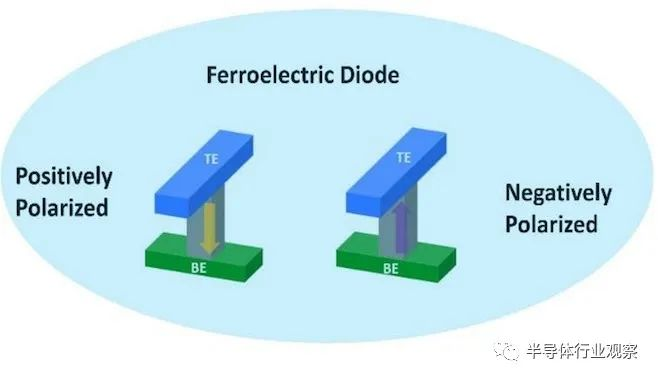
In addition to its operability as a storage cell, AlScN can be used to create ternary content addressable storage (TCAM) cells without transistors. TCAM cells are extremely important for big data applications, as searching for data using von Neumann architectures can be very time-consuming. Using a combination of LRS and HRS states, the researchers achieved an efficient tri-state parallel, all without the use of transistors.
Neural network using transistorless CIM arrays
To demonstrate the ability of AlScN to perform CIM operations, the UPenn group developed a convolutional neural network (CNN) using a FeD array. The array efficiently performs matrix multiplication by summing the output currents generated by the input voltage. The weight matrix (i.e., the relationship between the output current and the input voltage) can be tuned to discrete levels by modifying the conductivity of the cell. This tuning is achieved by biasing the AlScN film to exhibit the desired conductance.
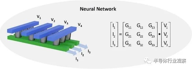
AlScN CNN successfully identifies handwritten digits from MNIST datasets using only 4-bit conductivity resolution, with a degradation of about 2% compared to 32-bit floating-point software. In addition, the absence of transistors makes the architecture simple and scalable, making it an excellent computational technique for future artificial intelligence applications requiring high-performance matrix algebra.
Breaking the von Neumann bottleneck

For most of its existence, AI computing has been primarily a software domain. However, as problems have become more data-intensive, the von Neumann bottleneck has had a deeper impact on the ability of systems to compute efficiently, making unconventional architectures more valuable. AlScN FeD-based analog CIM systems eliminate a major cause of latency in training and evaluating neural networks, making them easier to deploy in the field. The versatility of AlScN devices integrated with existing silicon hardware may provide a groundbreaking approach to integrating AI into more domains.
Original Article: Rethinking Computer Chips in the Age of Artificial Intelligence
Artificial intelligence poses a significant challenge to traditional computing architectures. In the standard model, memory storage and computation occur in different parts of the machine, and data must be moved from its storage area to the CPU or GPU for processing. The problem with this design is that moving takes time, too much time. You can have the most powerful processing unit on the market, but its performance will be limited because it will wait for data, a problem known as a “memory wall” or “bottleneck”.
When computational performance outperforms memory transfer, latency is inevitable. These latencies become a serious problem when dealing with the large amounts of data necessary for machine learning and artificial intelligence applications. As AI software continues to evolve and the rise of the sensor-intensive Internet of Things generates ever-larger data sets, researchers have focused on hardware redesign to deliver needed improvements in speed, agility, and energy use. A group of researchers at the University of Pennsylvania’s School of Engineering and Applied Science, in collaboration with scientists at Sandia National Laboratories and Brookhaven National Laboratory, has introduced a computing architecture well-suited to artificial intelligence. The project is co-led by Deep Jariwala, assistant professor in the Department of Electrical and Systems Engineering (ESE), Troy Olsson, associate professor of ESE, and Xifen Liu, Ph. A candidate for the Jarawala Device Research and Engineering Laboratory, the research team relies on an approach called in-memory computing (CIM).
In the CIM architecture, processing and storage occur in the same place, thereby eliminating transfer times and minimizing energy consumption. The team’s new CIM design, the subject of a recent study published in Nano Letters, is notable for being completely transistorless. The design is uniquely adapted to the way big data applications change the nature of computing. “Even when used in an in-memory computing architecture, transistors affect data access times,” Jariwala said. “They require extensive wiring throughout the chip’s circuitry and therefore use more time, space and energy than we expect for artificial intelligence applications. The beauty of our transistorless design is that it is simple, small, fast, and requires very little energy.” The architecture’s advances are not only in the circuit-level design. This new computing architecture builds on the team’s earlier work in materials science, which focused on a semiconductor called scandium alloy aluminum nitride (AlScN). alScN allows ferroelectric switching with physical properties that are faster and more energy efficient than alternative non-volatile storage elements.
“A key property of this material is that it can be deposited at temperatures low enough to be compatible with silicon fabricators,” Olsson said. “Most ferroelectric materials require much higher temperatures. the special properties of AlScN mean that the storage devices we are demonstrating can be on top of a silicon layer in a vertically heterogeneous integrated stack. Think of the difference between a multi-story parking garage for a hundred cars and a hundred individual parking spaces spread over a single plot. Which is more efficient in terms of space? The same is true for information and devices in highly miniaturized chips like ours. This efficiency is just as important for applications that require resource constraints, such as mobile or wearable devices, as it is for applications that are extremely energy intensive, such as data centers.”
In 2021, the team established the viability of AlScN as an in-memory computing powerhouse. Its capabilities in miniaturization, low cost, resource efficiency, ease of manufacturing and commercial viability have made significant advances in both research and industry.
In a recent study that debuted a transistorless design, the team observed that their CIM ferrodiode may execute up to 100 times faster than traditional computing architectures.
Other research in the field has successfully used in-memory computing architectures to improve the performance of AI applications. However, these solutions are limited in their ability to overcome the conflicting tradeoffs between performance and flexibility. Computational architectures using memristor cross arrays, a design that mimics the structure of the human brain to support the advanced performance of neural network operations, have also demonstrated admirable speedups. However, neural network operations using multilayer algorithms to interpret data and recognize patterns is only one of several key classes of data tasks required for functional AI. The design is not sufficiently adaptable to provide adequate performance for any other AI data operations. The Penn team’s iron diode design provides breakthrough flexibility not found in other in-memory computing architectures. It achieves superior accuracy and performs equally well in the three fundamental data operations that form the basis of effective AI applications. It supports on-chip storage, or the ability to hold the massive amounts of data needed for deep learning, parallel search, a feature that allows precise data filtering and analysis, and matrix multiplication acceleration, the core process of neural network computing.
“Suppose,” Jariwala said, “you have an AI application that needs large memory for storage and the ability to do pattern recognition and search. Think of self-driving cars or autonomous robots that need to respond quickly and accurately to dynamic, unpredictable environments. With traditional architectures, you need to use a different area of the chip for each function, and you can quickly run out of availability and space. Our ferro-diode design allows you to program it by simply changing the applied voltage to do all the work in one place.” The payoff of a CIM chip that can accommodate multiple data manipulations is clear: When the team ran simulations of machine learning tasks through their chip, it executed with an accuracy comparable to AI-based software running on a traditional CPU.
“This research is important because it demonstrates that we can rely on in-memory technology to develop chips that integrate multiple AI data applications, thus truly challenging traditional computing techniques,” said Liu, the study’s first author. The team’s design approach takes into account that artificial intelligence is neither hardware nor software, but rather an essential collaboration between the two. “It’s important to realize that all AI computing done today is software enabled on silicon hardware architectures designed decades ago,” Jariwala said. “That’s why AI as a field has been dominated by computer and software engineers. Fundamentally redesigning AI hardware will be the next big change in semiconductors and microelectronics. We are now heading toward software and hardware co-design.” “We design hardware that allows software to work better,” adds Liu, “and with this new architecture, we ensure that the technology is not only fast but accurate.”
Edited by Fei Huang