When we say that an Integrated Circuit (IC) package is “mature,” we mean that it is versatile and can provide a wide range of functions. That description aptly fits PDIP, one of the IC packages built using a through-hole process.
If you have been meaning to learn more about how it works, this blog post explains everything you need to know.
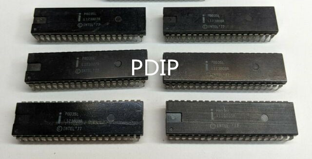
What is PDIP?
PDIP is Plastic Dual In-Line Package. It is one of the many IC packages categorized under Dual In-Line Package (DIP).
It is described as being “mature” because of the high-resistance to moisture, a factor that could have contributed to the package’s wearing out faster if it weren’t there.
Here are so many other things you need to know about the PDIP.
General Body Design
As the name signifies, PDIP is made of plastic. To put it in perspective, most of the Dual In-Line Packages (DIPs) for Printed Circuit Boards (PCBs) are either made from an opaque molded plastic.
Besides, the plastic is typically pressed into a lead frame made from either tin, gold or silver.
PDIP is Made from Drilling Technology
Several types of protective packaging technologies exist, with each of them offering a wide range of configuration options. The most popular ones are Surface Mount Technology (SMT), Chip Carrier and Through-Hole Technology (THT). The PDIP package uses the latter.
PDIP’s through-hole technology allows for drilling to be made on the package from where the semiconductor components would be mounted on the circuit board.
One important attribute of the Through-Hole Technology (THT) is the soldering of the component’s leads to the exposed pads on the Printed Circuit Board (PCB). From here, the leads would either be connected to the PCB electrically or mechanically.
Body Dimensions and Lead Spacing
Dual In-Line IC Packages (DIPs) tend to maintain a convenient spacing, allowing other pins or leads to be integrated on the circuit board. the Plastic Dual In-Line Package (PDIP) toes the same line by maintain a dual body dimension of 300 mils and 600 mils.
As for the lead or pin count, it can move from 8 to 64, depending on the package’s configurations.
The major downside to the wider spacing between the two rows or two sets of in-line pins formed via the leads extending from both sides is the maximum pin count. Due to the larger spacing of up to 2.54mm lead pitch, it becomes practically impossible to fit in multiple leads into the package.
That informs the reason why the pin range of the PDIP can be anywhere between 8 and 64, with some of the packages’ pins being as low as 16 and 28.
Low-Cost Variant of DIPs
One of the major advantages of working with the Plastic Dual In-Line Packages (PDIPs) is the cost-effectiveness. Due to the plastic coverage, the costs of manufacturing the package are lower than those made from ceramics.
Features of the PDIP
The following are some of the integral properties of the Plastic Dual In-Line Package (PDIP):
1. Moisture Resistance
Moisture getting into the Printed Circuit Board (PCB) potentially limits the board’s capabilities. Using the PDIP with its plastic enclosure. The most outstanding attribute here is the use of two halves of the package and either fusing or cementing them together.
By doing this, the package is able to keep out most contaminants. The higher protection against contaminants is provided via the provision of air and moisture that tightens the sealed leads while protecting the Integrated Circuit (IC) die inside the package.
2. PDIP has a Smaller Variant
Working with the Plastic Dual In-Line Package (PDIP) keeps out the contaminants and provided the package is kept in a controlled environment, it can last for many years.
However, your options are not limited to the PDIP. You can also get the more portable or “shrunk” variant called the SPDIP.
With the full name as Shrink Plastic Dual In-Line Package (SDPIP), it provides the smaller variant of the PDIP. This denser version of the PDIP has a lead pitch of 1.778mm.
3. Name Variants
The PDIP is known with many other names, including Molded Plastic Dual In-Line Package (MPDIP) and Molded DIP. So, don’t be confused when you see the names interchanged – they basically mean the same thing.
4. Higher Conductivity
PDIP has a higher thermal or heat conductivity, which makes it one of the best IC packages to use when working on an application requiring excellent heat dissipation.
We would like to mention that the package’s higher thermal capability is derived from the copper lead frame, of which Copper (Cu) is one of the materials with a higher thermal property.
5. Non-Static Tubes
Plastic Dual In-Line Packages (PDIP) are typically packaged in a 20-inch anti-static tubes, further improving the versatility of the package during the integration to the PCB.
Downside to Working with the Plastic Dual In-Line Package (PDIP)

Have in mind that some potential drawbacks are tenable when working with the PDIP IC package. You want to have the following in mind:
1. Bond Breakage
The single bond wire holding the package is susceptible to breakage. Its breaking is possible because of the upward loop design of the bond. One more thing – the wire bond may break or detach if the materials get in touch with it.
Either way, the breakage or detachment of the wire bond can render the Integrated Circuit (IC) useless.
2. PDIP can be Expensive
Although the Through-Hole Technology (used on the PDIP IC package) is popular, it is expensive, when compared to the Surface Mount Technology (SMT).
Therefore, if you are looking to save a considerable amount of money when using an IC package, the THT may not be a cost-effective option.
3. A Higher Degree of Hermeticity is not Achieved with the PDIP
Although the package seals the plastic halves around the leads to prevent moisture, it lacks in some areas.
Its hermeticity level is lower, because of the package’s overt exposure to moisture. Besides, it is not known for certain if the cemented plastic halves can bolster the microscopic seal between the plastic in the package and the leads around the package’s perimeter.
Final Words
Plastic Dual In-Line Package (PDIP) has the leads protruding to the other side of the Printed Circuit Board (PCB) once mounted. You however want to consider the weight, which is bulkier than the modern variants of the Dual In-Line Packages (DIPs).
For that purpose, going for the Shrink Plastic Dual In-Line Package (SPDIP) may be a better option, because of the lighter bulk and massive real estate.