
Terahertz radiation, with wavelengths between microwave and visible light, can penetrate many non-metallic materials and detect the characteristics of certain molecules. These properties can be used for a variety of applications, including airport security scanning, industrial quality control, astrophysical observations, nondestructive characterization of materials, and wireless communications with bandwidths higher than the current cellular frequency band.
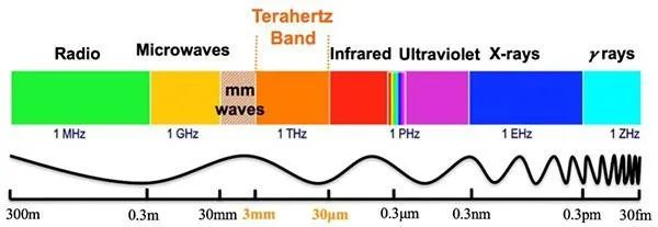
Figure 1 Position of terahertz in the electromagnetic spectrum
So many applications, can not be achieved without terahertz imaging technology, through various types of terahertz detectors to obtain terahertz waves and objects after the action of the signal, combined with image processing algorithms to get a complete image that can reflect the internal defects of objects, foreign bodies and various types of structural representation, is an important prerequisite for the application of terahertz technology in nondestructive testing, security inspection. Therefore, terahertz detectors have been a hot topic of research for scientists, especially the development of detection chips with high detection sensitivity, fast response time, room temperature operation, and easy integration of ultra-large-scale arrays (multi-image elements) is of great scientific significance and practical application value.
ONE
Terahertz camera for microbolometer thermal radiometer
Currently, it has been challenging to design devices for detecting terahertz waves and producing images, such as cryogenic superconducting detectors with high sensitivity, but the devices are expensive, slow, bulky, and require vacuum systems and extremely low temperatures. Another class of equipment for room temperature detection imaging uses the microbolometer (microbolometer) principle. Based on the photothermal effect of terahertz microbolometer has the advantages of room temperature imaging, real-time imaging, simple and easy to carry and compatible with infrared microbolometer structure, process and so on. The basic working principle is that the terahertz radiation incident to the microbridge structure makes the thermistor layer temperature change, which causes the thermistor layer resistance to change, and generates the corresponding electrical signal output under the action of the applied bias, and finally reduces to image information.
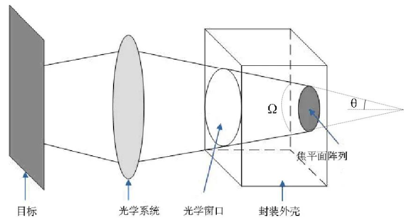
Figure 2 Principle of microbolometer in which the design of microbridge structure is a key factor affecting the performance of microbolometer. 2005 Alan W.M. Lee et al. of MIT proposed continuous wave terahertz transmission imaging based on VOx focal plane detector, which used BAE System SCC 500L VOx focal Plane detector assembly with 160×120 image elements and 46um×46um image element size was used to achieve 2.52THz continuous wave transmission imaging.

Like, demonstrating the feasibility of using microbolometer as a terahertz detector
The conventional microbridge structure has low sensitivity and low resolution when used in the terahertz band due to the lower energy and longer wavelength of terahertz radiation compared to infrared radiation. In order to improve the absorption efficiency of the microbridge structure for terahertz radiation, new microbridge structures must be designed, such as changing the single-layer structure to a double-layer microbridge structure or changing the bridge leg structure, etc. In 2008, NEC Corporation of Japan increased the absorption rate of the microbridge for terahertz radiation by adding a metal absorber layer to the top layer of the conventional VOx thermal material-based microbridge structure. The detection rate of terahertz radiation using this structure is higher than that of conventional junction.
There is a certain improvement in terms of structure.
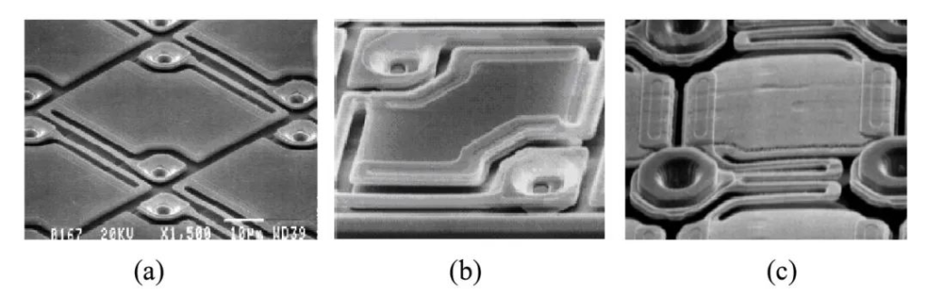
Fig. 4 (a) “I-type” bridge leg; (b) “L-type” bridge leg; (c) improved structure Because the microbolometer array process in the terahertz band is compatible with the infrared camera, it is the first chip to implement a terahertz camera, and it is also the mainstream of terahertz cameras being developed. research and development of terahertz cameras in the mainstream. There are already well-known foreign companies in the industry have launched mature
Technologies such as field-effect-tube based detector arrays and quantum-well (QW) based multi-image detector arrays are also hot spots for research. Many domestic research institutions are dedicated to the localization of terahertz array detectors, for example, the Suzhou Institute of Nanotechnology, Chinese Academy of Sciences has realized the array of transistor mixing detectors, and the Shanghai Institute of Microsystems and Information Technology has made many breakthroughs in quantum well detectors, but they have not been fully commercialized yet.
TWO
Latest Research – Quantum Dot Terahertz Camera
Recently, researchers at MIT, the University of Minnesota and Samsung have developed a new type of camera that can detect terahertz pulses quickly and with high sensitivity at room temperature and high voltage. More importantly, it can simultaneously capture information about the direction or “polarization” of the wave in real time, which is not possible with existing devices, and which can be used to characterize materials with asymmetric molecules or to determine the surface shape of materials.
The new system uses quantum dots that emit visible light when stimulated by terahertz waves, which can be recorded by a device similar to a standard electronic camera detector and can even be seen with the naked eye. MIT doctoral student Jiaojian Shi, chemistry professor Keith Nelson and 12 others described the device in a paper published Nov. 4 in the journal Nature Nanotechnology.
The team produced two different devices that can operate at room temperature: one uses the ability of quantum dots to convert terahertz pulses into visible light, allowing the device to produce images of materials; the other produces images showing the polarization state of terahertz waves. The new “camera” consists of several layers made using standard manufacturing techniques, such as those used for microchips. A series of nanoscale parallel gold wires, separated by narrow slits, are located on the substrate; on top is a layer of light-emitting quantum dot material; on top is the CMOS chip used to form the image. Polarization detectors, called spinners, use a similar structure but have nanoscale annular slits that allow them to detect the polarization of the incident beam

Figure 7 Schematic diagram of the qTV CMOS terahertz camera and spinner. The device consists of a field-enhanced structure (nano-slit or nano-coaxial) coated with quantum dots and a CMOS camera. The inset shows the conversion of terahertz photons into visible photos by field-driven charge transfer between the quantum dots, followed by radiative recombination at the end of the terahertz pulse.
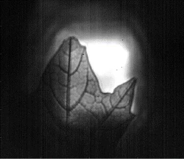
The photon energies of terahertz radiation are extremely low, which makes them difficult to detect. So what this device is doing is converting tiny photon energies into something visible that can easily be detected with an ordinary camera. In the team’s experiments, the device was able to detect terahertz pulses at low intensity levels that exceed the capabilities of today’s large and expensive systems. The researchers demonstrated the sensitivity and resolution of the system by taking terahertz illumination photographs of some of the structures used in their device to demonstrate the functionality of the detector, such as the nanospaced gold wires and ring slits used in the polarization detector.
