Operational amplifiers are versatile and can be used to build a variety of circuits with many uses. This is an introduction to a differential amplifier circuit made from an operational amplifier.
For a differential amplifier circuit, both the forward and reverse phase inputs require a signal source, which can be either a stable and constant voltage or a signal with variable voltage amplitude, which is processed by the differential circuit to give the difference between the two input sources.
The difference amplifier amplifies the difference between the two voltages, thus making this type of operational amplifier circuit a subtractor, rather than adding or summing the input voltages as a summing amplifier would.
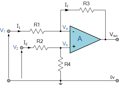
Differential amplifier circuit principle: this still relies on the op-amp virtual short and virtual break principle to push.
The voltage at the inverting end of the op-amp and the positive phase input are always equal;
False break: no current input at the inverting and forward inputs of the op-amp;

According to the false short principle, Va = Vb , according to the false break principle and the total circuit current sum is 0, I1 = If.
And according to the voltage division principle Vb = V2*R2/(R2+R4) ,
I1=If => V1/R1 =Va-Vout/R3=Vb-VOUT/R3.
Introduce the Vout equation:
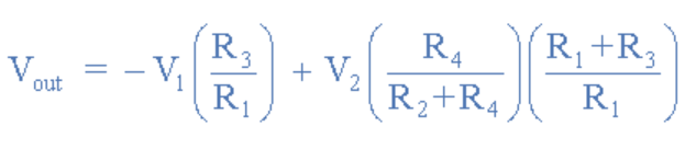
When R1 and R2 choose the same value, R3 and R4 choose the same value, the formula becomes: Vout = R3/R1 (V2-V1), from the formula can be seen that the difference is a principle of subtraction, R3/R1 is the gain of the amplifier.
If R1, R2, R3 and R4 are all of the same resistance, then Vout =V2-V1, which is directly the difference between the positive and negative phase values of the input.
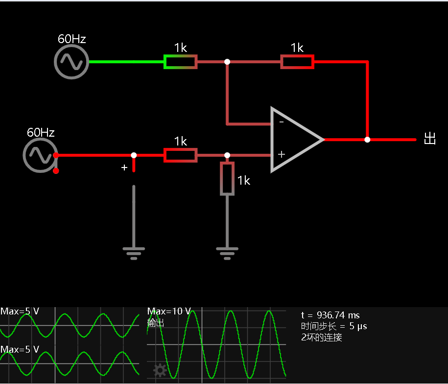
In order to understand this principle process more clearly, the simulation software is used to understand it in detail.
In the following simulation procedure, a sine wave with the same voltage amplitude and opposite phase is input to the positive and inverting inputs respectively, with R1, R2, R3 and R4 all taking the same value. Then the minimum phase reduction at the trough of the waveform is -10V and the maximum phase reduction at the crest is 10V.