IC designing or integrated circuit design is included as a part of the larger knowledge which is referred to as electronics engineering. Here in this discipline, we have a process called circuit design. Circuit design has a major goal, which is assembling some elements of interconnected circuits, which performs a particular objective function. In addition, this ability to multiply as well as add numbers is one easy and simple example.
Circuit elements that are useful in the process starts with basic building blocks like wires, capacitors, resistors, and transistors. The combination of these elements help in the formation of functions that are more complex like precision amplifiers. It also includes logic gates that are combined to create other complex functions like multipliers and adders. The process goes on to build more on itself. Therefore this leads to the presence of more circuit building blocks that are complex.
IC designing makes use of pre-manufactured and discrete elements in forming the circuit. Regarding IC designing, there is a significant difference. For this case, the manufacturing of these circuit elements are from implemented miniaturized components on the silicon substrate. This makes use of a process referred to as photolithography. Furthermore, the process of photolithography helps in creating different geometric shapes on that silicon substrate. Here, there is an alteration on the region’s electrical properties that the shape defines. The creation of the fundamental circuit elements happen when you combine, as well as superimpose over themselves.
Therefore, IC designing is made up of two main processes. The first is the assembling of the circuit elements in order to perform the main function. Also, after this, you need to assemble and interconnect the different geometric shapes implementing these circuit elements on your silicon substrate.
What is the Importance of IC Designing?
IC designing is known as an important discipline. This is a very important part that aids the developing of virtually all the microelectronic devices that are in use as of today.
This has to do with the microprocessors powering cell phones and laptop computers. These also include image processing circuits, which help in the powering of television sets and computer monitors, as well as sensors, which are useful in implanted and wearable medical devices
Also, the microelectronic devices permits the increasing use of AI (artificial intelligence), which is opening some new frontier like machine vision, autonomous driving, and natural language processing. The deployment of IC technology has also become well-known globally, as well as IC design helps in forming the basic set of disciplines that are necessary in creating the devices.
What are the Steps Involved in IC Designing Flow?
The IC designing process could be thought of as some steps of hierarchical decomposition. The decomposition of the high-level requirements is done into additional details having the specific goal of integrating a circuit on the silicon wafer, which performs the main and objective function. These main steps, which make up IC designing, include the following.
Architectural Design
This is the place where you specify the integrated circuits required functionality. You will consider the IC capabilities that are contemplated with respect to the system that is being built.
Now, what function must the integrated circuit offer or deliver? Also, what power consumption and speed is required? Furthermore, what is the device’s target cost? Whatever answers you give to the questions tells the subsequent choices you need for the technology, which is useful in implementing the device
Logic and Circuit Design
The assembling and interconnection of the building blocks at the macro-level is to help in implementing the necessary functionality of the integrated circuit.
Typically, it uses already existing building blocks like sensors, processing units, and memories. Functional descriptions (high-level) of the circuit boards are well decomposed in the low level circuit elements. Logic synthesis is the software that helps in automating the process.
In addition, the stimulation of these devices helps in the verification of the design’s functionality.
Physical Design
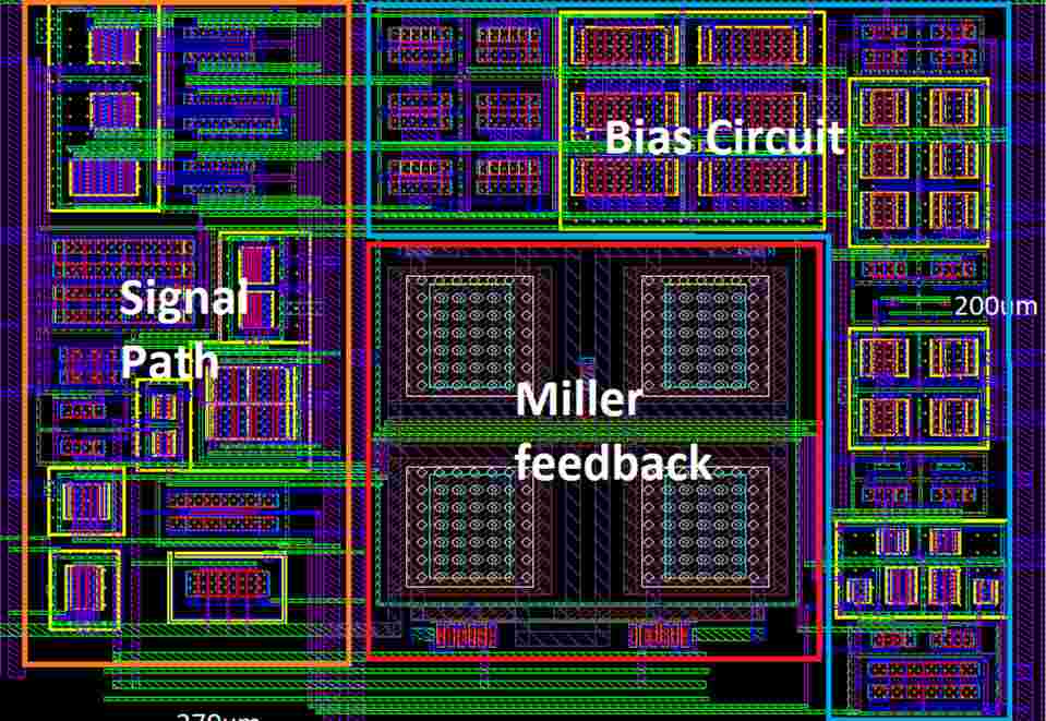
At this step o ic designing, the creation of the layout of these interconnected shapes, which implements all the necessary circuit elements present on the silicon wafer occurs. This process starts with a “floor plan” for the chip that explains where each of the chip’s primary functions will be, as well as where the design’s primary output and input ports will be.
To prepare for manufacturing, you then place the final elements of the circuit and then route them. Also, if there is a need to modify the building blocks (macro-level) to help in achieving the Integrated circuit’s requirements, you will use custom layout techniques, and make use of the integrated circuit layout editor. With this, you will define the way you should implement the chip.
Physical Verification
Note that you can model all the effects which the process of manufacturing usually adds onto the design. The added resistance gotten from signal crosstalk, wiring, as well as the variability in the process of manufacturing are some out of many items you must consider in this step of ic designing.
Now, will you circuit still function well when made to pass through these stresses? Furthermore, there are lots of design rules concerning the way you lay out the circuit physically on your silicon wafer in order to make sure that it can be manufacturable. At this particular step, make sure that you check the design rules properly.
Signoff
Signing off is the last step of ic designing before you send the design for manufacturing. This way, the important parameters that will have an effect on the chip’s manufacturability or performance will be verified and checked against the quality tools.
Furthermore, at this step, the full verification of the design rules takes place coupled with the rules for design for manufacturability. Here, you will also verify and close the signal integrity, power consumption, and the timing of that design.
Also, it is very important that you perform proper parasitic extraction all through the signoff. This is to make sure that the physical effects involved in the whole process are properly understood.
Conclusion
When considering IC designing, there are a lot of things to put in place. For advanced manufacturing, process variability and physical effects play a very important role.