The determination of detailed design scenarios in ASIC design is very important. The same design can be implemented by others with 30% smaller area and 30% less processing time than you, which is where the value of the design engineer comes into play.
Any design is confusing at the very beginning, with complex scenarios and various couplings. What we have to do is to sort out all the scenarios and then figure out how to normalize them. Any task that feels impossible to do at the beginning can eventually find a solution. This would have seemed to be a world without laws, but humans just go on searching and discovering the laws of operation of this material world. Of course, even though the first version of the design took into account as many scenarios and implementation options as possible, there were still some poorly thought out and unreasonable implementations in the final implementation stage, and due to the time cost, it was decided to put it into the next version and modify it again. This process is called optimization! So, how to optimize a design?
Find a large register group
The first is to find a large register group in the design, the register is the basic unit of the larger area, the number of registers determines the overall area of the design order of magnitude. Small capacity storage with regfile, general register set used thousands of bits, we must consider whether to use RAM. tens of thousands of bits is unreasonable design. See the large register group is to focus on the optimization of the object, it should be noted that the register group is free to take the value in any bit, RAM is required to read a beat, so you need to do a compromise (trade-off) before the high parallelism and area. The data path register beat too much, certainly not reasonable, a data beat at least a few dozen bits, beat more than a beat, on hundreds of bits, and a design idea, in the control of how much logic, control signals + counters, do more than a few groups are also close to a few dozen bits. For example, the data and valid signal from the previous module, the data is to be used a few beats later, should be made before the first module to the valid signal, the data comes a few beats later, to avoid data beat. In the data path there are some combinations of logic path is not long, playing a beat, so although the timing will be better, but the final increase in area is not worth it, so the extra register beat can be completely “dry”.
Retiming
Retiming is to readjust the timing, for example, the circuit encountered in complex combinational logic, the delay is too large, the circuit timing does not meet, this time using pipelining technology, insert registers in the combinational logic plus pipelining, operation, area for speed ideas.
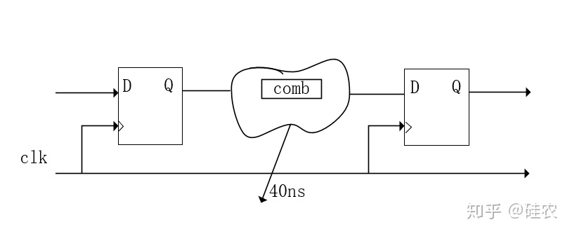
Any digital circuit can be equated to combinational logic plus D flip-flop beat, the combination of logic path between the two D flip-flops determine, the operating frequency of the system, determine the performance of the chip. So in order to improve the chip’s operating frequency, use pipeline technology to insert registers in the combinational logic.

Insert the location of the register needs to be carefully selected, the number of registers consumed by the beat of data in different locations is different, let’s say you consume 25bit registers in location a, location b consume 20bit registers, save as much as you can.

The position of the front inserted registers makes the delay of comb1 30ns and the delay of comb2 10ns. The maximum operating frequency of the system is determined by the longest path. That means the period of the highest operating frequency of your system, not less than 30ns, is inserted in front of the pipeline, this time we do not change the timing, using retiming technology, so that the delay between the various combinational logic is equivalent.
Crazy multiplexing
Find the same unit of computational logic, reuse the most common is the counter, can be achieved with a counter, do not use two, the same logic between the underlying modules try to use a piece of circuitry to reduce duplication of design. Example of sharing basic logic units, area: adder > comparator > selector. Adder than selector. Multipliers are essentially full adders as well. So there is select then compare, select then add, select then multiply. Draw a diagram to mean it.

The adder here can be replaced with any logic or module.
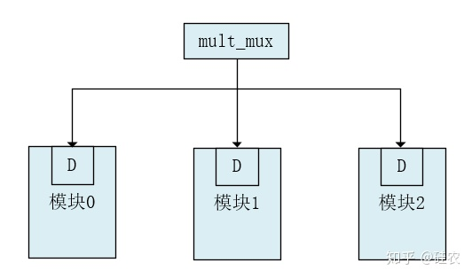
Multiplier timeshift reuse degree increase
In the calculation module multiplier is also a very large part of the logic, a design to consider the optimal PPA, we must consider the number of multipliers and how much reuse can be maximized, the pursuit of the best design is the entire data path in the multiplier idle not down. The multiplier call method is generally used when the input of the multiplier guarantees the register input and the result is output to each multiplexer module with a beat. It can be made to beat after the multiplication operation is performed, so that the registers consumed will be much less. Draw a diagram to mean it (single bit).
Before modification
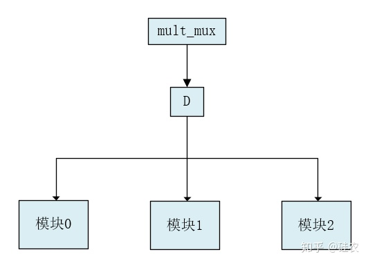
After modification, the registers are saved a lot, but the output register load of multiplier will become larger, but the back-end synthesis is constrained when max_fan_out tool will automatically insert buffer and copy registers, after actual testing or will save a lot of area, put some optimization work can be left to the tool to do, understand it, trust it, and use it.
RAM reuse
From the overall point of view of the design, RAM can also be reused, the front processing used ram, now empty, can be used later.
Finally
To summarize the design/optimization ideas for individual ASIC modules, list all the conditions, then normalize, reuse, and area and speed call out the ideas throughout. This piece is first organized here, see you in the next one.