fpga hardware design can be a difficult and costly process. However, with the right tools and workflow, it can be much easier and more affordable. In this blog post, we will discuss how to design fpga hardware, including tips on choosing the right tools and workflow for your project. By following these tips, you can save time and money while still getting the results you need. Thanks for reading!
Define the purpose of the fpga design. What does it need to do?
Designing fpga hardware is an important part of modern electronics. These integrated circuits often provide the backbone of systems that require speed, flexibility, and reliability. It is essential to define the purpose of the fpga design before any sort of development begins. The fpga has to do more than just fulfill its task -it should also adhere to criteria such as size, power consumption, cost, or other needs specific to the project’s goals. To determine these requirements and write a detailed design document is paramount for making sure that your fpga hardware does what it needs to do. Doing so will help ensure desired results and make for a successful fpga design in the end.
Choose the right fpga for the job. There are many different types and sizes available.
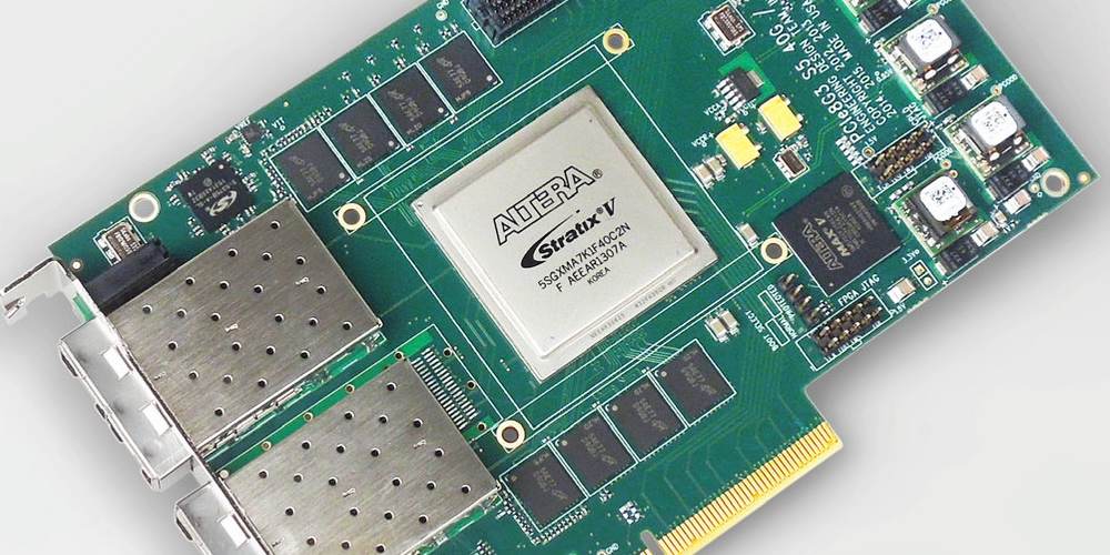
When looking for the perfect fpga hardware for a job, there are many traits to consider based on size, power, and capacity. This means that choosing the right fpga hardware is essential to ensure that your project will run smoothly. With a variety of fpgas on the market, finding the one that best fits your needs can seem like an intimidating process. But with the right research, you’ll be able to find exactly which fpga hardware can deliver the most efficient results for your next project.
Create a schematic of the design using a software program like CADENCE or OrCAD.
Designing fpga hardware requires an intricate understanding of the task being automated, as well as the integrated circuit and its components. In order to create a schematic for fpga design, software programs such as CADENCE or OrCAD must be utilized to visualize the project. CADENCE allows users to add points, lines, shapes, and other features in order to create a refined schematic of fpga hardware designs. Similarly, OrCAD offers tools that can further refine the fpga design using symbols and components. Once a schematic has been created using either software program, it can then be turned into reality with various tools commonly found in fpga design suites. Therefore, utilizing CADENCE or OrCAD is both essential and intuitive in designing fpga hardware.
Implement the design on the fpga by programming it with Verilog or VHDL code.
After a fpga hardware design has been determined, the implementation of the design requires a computer programming language to be used. Verilog and VHDL are both valid programming languages to use when designing fpga hardware. With these languages, you can generate detailed instructions that will direct the fpga in using its physical circuitry to create the desired fpga hardware design. Knowing how to properly program with these languages is key to successfully implementing your designs on fpga hardware.
Test the design to make sure it works as intended. Debug any errors that may occur.

Testing fpga hardware is an integral part of the design process as it allows engineers to detect any possible errors in their fpga system. It’s important to test the design in order to make sure that everything works properly and that all expectations for functionality and performance are met. Additionally, the debugging process can help locate and identify any issues within the fpga, allowing engineers to pinpoint and remediate any errors that occur. Testing fpga hardware is a must for ensuring proper design and function each time.
Designing fpga hardware can be a complex task, but it is possible to do with some careful planning and execution. By following the steps outlined in this article, you can create a functional and reliable design that meets your specific needs. With the right tools and an understanding of how fpgas work, you can achieve success in your fpga design projects.