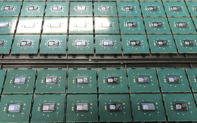
EP2S30F672C5N ApplicationField
-Cloud Computing
-5G Technology
-Internet of Things
-Consumer Electronics
-Artificial Intelligence
-Industrial Control
-Medical Equipment
-Wireless Technology
Request EP2S30F672C5N FPGA Quote , Contact Sales@ebics.net Now
EP2S30F672C5N FAQ

Q: How can I obtain software development tools related to the INTEL FPGA platform?
A: Quartus Prime Modelsim is the corresponding programming software for FPGA produced by Altera/Intel. The specific choice depends on personal habits and functional requirements to specifically select a more suitable match. You can search and download through the FPGA resource channel.
Q: What should I do if I did not receive the technical support for EP2S30F672C5N in time?
A: Depending on the time difference between your location and our location, it may take several hours for us to reply, please be patient, our FPGA technical engineer will help you with the EP2S30F672C5N pinout information, replacement, datasheet in pdf, programming tools, starter kit, etc.
Q: Do I have to sign up on the website to make an inquiry for EP2S30F672C5N?
A: No, only submit the quantity, email address and other contact information required for the inquiry of EP2S30F672C5N, but you need to sign up for the post comments and resource downloads.
Q: Does the price of EP2S30F672C5N devices fluctuate frequently?
A: The EBICS search engine monitors the EP2S30F672C5N inventory quantity and price of global electronic component suppliers in real time, and regularly records historical price data. You can view the historical price trends of electronic components to provide a basis for your purchasing decisions.
Q: Where can I purchase INTEL EP2S30 Development Boards, Evaluation Boards, or Stratix II FPGA Starter Kit? also provide technical information?
A: EBICS does not provide development board purchase services for the time being, but customers often consult about ZedBoard, Basys 3 board, TinyFPGA BX, Nexys4-DDR, Terasic DE10-Nano, Digilent Arty S7, etc. If you need relevant technical information, you can submit feedback information, our technicians will contact you soon.
Q: How to obtain EP2S30F672C5N technical support documents?
A: Enter the “EP2S30F672C5N” keyword in the search box of the website, or find these through the Download Channel or FPGA Forum .
EP2S30F672C5N Features
The Stratix II family offers the following features:
Request EP2S30F672C5N FPGA Quote , Contact Sales@ebics.net Now
EP2S30F672C5N Overview
Introduction
The Stratix® II FPGA family is based on a 1.2-V, 90-nm, all-layer copper
SRAM process and features a new logic structure that maximizes
performance, and enables device densities approaching 180,000
equivalent logic elements (LEs). Stratix II devices offer up to 9 Mbits of
on-chip, TriMatrix™ memory for demanding, memory intensive
applications and has up to 96 DSP blocks with up to 384 (18-bit × 18-bit)
multipliers for efficient implementation of high performance filters and
other DSP functions. Various high-speed external memory interfaces are
supported, including double data rate (DDR) SDRAM and DDR2
SDRAM, RLDRAM II, quad data rate (QDR) II SRAM, and single data
rate (SDR) SDRAM. Stratix II devices support various I/O standards
along with support for 1-gigabit per second (Gbps) source synchronous
signaling with DPA circuitry. Stratix II devices offer a complete clock
management solution with internal clock frequency of up to 550 MHz
and up to 12 phase-locked loops (PLLs). Stratix II devices are also the
industry’s first FPGAs with the ability to decrypt a configuration
bitstream using the Advanced Encryption Standard (AES) algorithm to
protect design.
Features
The Stratix II family offers the following features:
■ 15,600 to 179,400 equivalent LEs; see Table 1–1
■ New and innovative adaptive logic module (ALM), the basic
building block of the Stratix II architecture, maximizes performance
and resource usage efficiency
■ Up to 9,383,040 RAM bits (1,172,880 bytes) available without
reducing logic resources
■ TriMatrixmemory consisting of three RAM block sizes to implement
true dual-port memory and first-in first-out (FIFO) buffers
■ High-speed DSP blocks provide dedicated implementation of
multipliers (at up to 450 MHz), multiply-accumulate functions, and
finite impulse response (FIR) filters
■ Up to 16 global clocks with 24 clocking resources per device region
■ Clock control blocks support dynamic clock network enable/disable,
which allows clock networks to power down to reduce power
consumption in user mode
■ Up to 12 PLLs (four enhanced PLLs and eight fast PLLs) per device
provide spread spectrum, programmable bandwidth, clock switchover,
real-time PLL reconfiguration, and advanced multiplication
and phase shifting
■ Support for numerous single-ended and differential I/O standards
■ High-speed differential I/O support with DPA circuitry for 1-Gbps
performance
■ Support for high-speed networking and communications bus
standards including Parallel RapidIO, SPI-4 Phase 2 (POS-PHY
Level 4), HyperTransport™ technology, and SFI-4
■ Support for high-speed external memory, including DDR and DDR2
SDRAM, RLDRAM II, QDR II SRAM, and SDR SDRAM
■ Support for multiple intellectual property megafunctions from
Altera MegaCore® functions and Altera Megafunction Partners
Program (AMPPSM) megafunctions
■ Support for design security using configuration bitstream
encryption
■ Support for remote configuration updates
The INTEL Embedded – FPGAs (Field Programmable Gate Array) series EP2S30F672C5N is FPGA, STRATIX II, 30K ELEMENTS, FBGA672, View Substitutes & Alternatives along with datasheets, stock, pricing from Authorized Distributors at EBICS.com,
and you can also search for other FPGAs products.
EP2S30 development board
Stratix II FPGA evaluation kit
EP2S30 reference design
INTEL Stratix II FPGA development board
EP2S30F672C5N Datasheet PDF
INTEL EP2S30
Stratix II FPGA EP2S30
Stratix II FPGA starter kit
EP2S30F672C5N TechnicalAttributes
-Number of I/Os 500
-Minimum Operating Temperature 0 C
-Number of Logic Blocks 1694
-Package / Case FBGA-672
-Maximum Operating Temperature + 70 C
-Operating Supply Voltage 1.2 V to 3.3 V
-Packaging Tray
-Series Stratix II
-Operating Supply Current 0.3 A
-Distributed RAM 1.4 Mbit
-Series Stratix II
Request EP2S30F672C5N FAQ Quote , Pls send email to Sales@ebics.net or Submit form now
Related posts:
- XCVU440-2FLGA2892E XCVU440 reference design XCVU440-2FLGA2892E Datasheet PDF
- XCVU160-3FLGC2104E XCVU160 evaluation board XCVU160-3FLGC2104E Datasheet PDF
- XCVU125-2FLVC2104E Xilinx XCVU125 Virtex UltraScale FPGA evaluation kit
- A54SX72A-1FGG484I A54SX72A reference design A54SX72A-1FGG484I Datasheet PDF

