A preamble
Electronic products can not work without power supply, with the development of the electronics industry, power supply DC-DC module is also increasingly towards the direction of small size, high efficiency, low power loss, switching frequency becomes high.
But the switching power supply DC-DC module electromagnetic interference (EMI), has always been a major constant in the field of electromagnetic compatibility (EMC), so the DC-DC module EMI noise suppression must be paid attention to, so as to improve the performance and quality of electronic products, so that it successfully passed the EMC standard certification.
Today we share a set of DC-DC power supply rectification combination!
Two noise generated by the causes
Power switch DC-DC work, the source of noise generated by the source can be attributed to two main points.
- noise caused by the switching frequency of the switching tubes when the module is working.
- module work due to resonance caused by the resonance of the parasitic inductance and capacitance in the switching loop caused by the ringing voltage caused by noise.
Paths of noise transmission.
- radiation: noise is radiated to space in the form of electromagnetic waves through the loop formed by the IC and the cable (the larger the loop area the stronger the radiation).
- conduction: noise in the form of differential mode and common mode noise transmitted through the cable to the higher-level devices and lower-level devices.
The following take a simple buck circuit topology diagram to show you the specific loop of noise, the following figure, the red part of the parasitic inductance and parasitic capacitance, they are the cause of resonance in the loop.
- state (1), when switch 1 is open, switch 2 is closed buck circuit noise through the input decoupling capacitor and the upper switch tube then flow input filter capacitor and then back to the decoupling capacitor ground to form a loop, as follows.

State (1) noise loop diagram
- State (2), when switch 2 is open and switch 1 is closed the noise from the buck circuit flows through the switch down tube (external current-continuing diode) and then back through the output filter capacitor to form a loop, as follows.

State (2) noise loop diagram
Three methods of noise suppression
Through the analysis of the causes of noise generation, the following noise suppression methods and corresponding measures can be summarized.
(1) Optimize the noise return path and reduce the circuit area.
a. Add capacitors of different pF values at the input and output terminals, and high-frequency capacitors should be placed close to the input and output terminals.
b. Capacitors and ICs are placed on the same PCB layer.
c. Capacitor ground should be linked with chip ground at the shortest distance.
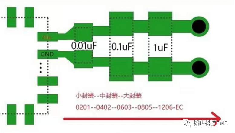
Reasonable capacitor placement diagram
(2) Suppressing noise conduction in the input-output path: adding appropriate magnetic beads at the input for isolation; adding common mode inductor filtering at the port.
(3) Cut the ringing amplitude of the switching frequency: add RC absorption circuit between the chip SW pin and the current-continuing diode within the acceptable power loss range.
(4) Optimize the PCB layout to reduce the circuit path area: the current-continuing diode should be close to the chip end; the lower end of the inductor should be hollowed out on the same layer.

Recommended PCB layout planning diagram
Four Classic Case Sharing
Next, we will share a classic case of EMC problem of power module. The following figure is the charging module circuit of a product, which exceeds the RE test in charging mode.
Let’s take a look at the spectrum chart of the test before rectification, as follows.

Test data before rectification
(a) Through the analysis of the waveform, it is clear that the waveform is a noise overload caused by the classic switching frequency.
Next, let’s look at the layout of the charging chip of the product, as follows.

Figure 1 Charging chip PCB front view
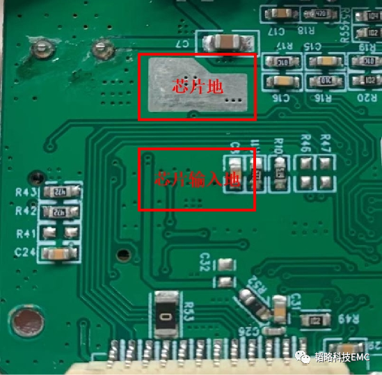
Figure 2: Back side of the charging chip PCB
The analysis of the circuit shows that the use and layout of the devices are still reasonable. However, the most obvious and fatal problem here is at the input side of the chip. The ground of the input decoupling capacitor marked with a red box in the first PCB diagram is connected to the ground on the bottom of the PCB by punching a hole, but this ground is not linked to the ground of the chip, but to other alignments to separate it, so the noise path back to the chip becomes longer and the return path becomes larger, as shown in Figure 2.

Corrective measures: use a piece of copper foil to lap up the chip and input ground, to provide a shorter path to the noise return, reducing the return area.
Next, let us look at the corrected test spectrum.

Test data after rectification
The noise has improved significantly and can pass the test standard.
V Summary
Power supply noise is an inseparable topic in the process of EMC rectification, and today we share it with the buck circuit, and the analysis of other modes of power supply circuit is also based on the gourd.