An operational amplifier is an IC (integrated circuit) which is a DC-coupled high-gain voltage amplifier with differential i/p and a single o/p. In this configuration, the o/p potential generated by an operational amplifier is typically many times greater than the potential difference between its i/p terminals.
Operational amplifiers have their origins in analogue computers and are used to perform mathematical operations in multiple linear, non-linear and frequency-dependent circuits. The popularity of this IC as a basic building block in analogue circuits was due to its flexibility. Today, operational amplifiers are the most commonly used integrated circuits. Applications for these ICs include a large number of industrial, scientific and consumer devices.
The operational amplifier is a type of differential amplifier that is used in a wide range of applications. IC 741 is a look at a general purpose operational amplifier model that looks like a small chip but is very useful, this article takes a look at it.
Basic concept
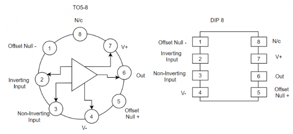
The 741 IC operational amplifier consists of eight pins, and the most important pins 2,3 and 6, where pins 2 and 3 indicate the inverting and non-inverting terminals, and pin 6 indicates the output voltage.
The IC 741 consists of various stages of transistors, usually with three stages such as differential i/p, push-pull o/p and intermediate gain stages, whose main function is to perform mathematical operations in various circuits.
The IC 741 offers a high range of voltage gains and can operate at a variety of voltage levels, and this function allows the device to be implemented in various integrators, summing amplifiers, etc. It even has the characteristics of a protection device in the event of a short circuit and has an internal network of frequency compensation circuits. The IC is available in three forms, namely an 8-pin SOIC package, an 8-pin double in-line package and an O5-8 metal package.
The IC 741 operational amplifier is available in both inverting (-) and in-phase (+) use.
Pin Configuration
The pinout of the IC 741 op-amp is shown below, where the function of each pin is explained in the following section.
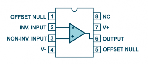
Power supply pins: pins 4 and 7; pins 4 and 7 are the positive and negative voltage supply terminals respectively, from which the power required to operate the IC is received. The voltage level between these pins can be in the range of 5-18V.
Output pins: Pin 6; the output of the IC 741 operational amplifier is received from this pin. The output voltage received at this pin is based on the feedback method used and the voltage level of the input pins. When the voltage value on pin 6 is high, this corresponds to an output voltage similar to the +ve supply voltage. Similarly, when the voltage value on pin 6 is low, this corresponds to an output voltage similar to the -ve supply voltage.
Input pins: Pin 2 and Pin 3; these are the input pins of the op-amp. Pin 2 is considered as an inverting input, while pin 3 is considered as a non-inverting input pin. When the voltage value on pin 2 > the voltage value on pin 3, i.e. when the voltage value on the inverting input is high, the output signal is low. Similarly, when the voltage value on pin 3 > the voltage value on pin 2, i.e. when the voltage value on the in-phase input is high, the output signal is high.

Offset zero pins: pin 1 and pin 5; as mentioned earlier, this op-amp has a higher voltage gain level. So even the smallest changes in the voltage at the non-inverting and inverting inputs due to anomalies in the construction process or other anomalies can have an effect on the output, and to overcome this it is necessary to apply a voltage offset value on pins 1 and 5, which is usually done by a potentiometer.
Unconnected pin: Pin 8; it is simply a pin used to fill the empty pins in the IC 741 op-amp. It is not connected to any internal or external circuitry.
Operating principle
A typical IC 741 consists of a circuit containing 11 resistors and 20 transistors, all of which are integrated and connected as a single chip. The diagram below makes it easy to understand the internal connections of the components.
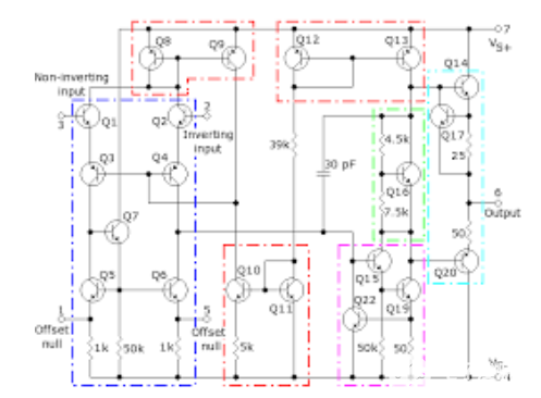
In the diagram above, for transistors Q1 and Q2, the inverting and in-phase inputs are connected in correspondence. transistors Q1 and Q2 are both used as NPN emitters, where these outputs are connected to a pair of Q3 and Q4 transistors. These Q3 and Q4 operate as common base amplifiers. This type of configuration isolates the inputs connected to Q3 and Q4 and therefore eliminates any signal feedback that may occur.
Voltage fluctuations occurring at the input of the operational amplifier may affect the internal circuit current and also the effective functional range of any transistors in the circuit. Two current mirrors have therefore been implemented to eliminate this from occurring. The transistor pairs (Q8, Q9) and (Q12, Q13) are connected to form a mirror circuit.
As the transistors Q8 and Q12 are regulation transistors, they set the voltage level at the EB junction for the corresponding transistor pair. This voltage level can be adjusted precisely to the decimal point of a millivolt and this precision allows only the necessary current to flow into the circuit.
A mirror circuit formed by Q8 and Q9 is fed to the input circuit, while another mirror circuit formed by Q12 and Q13 is fed to the output circuit. In addition, a third mirror circuit, formed by Q10 and Q11, is used as an added impedance connection between the -ve supply and the input. This connection provides a reference voltage level indicating no load effect on the input circuit.
Transistor Q6 together with 4.5K and 7.5K resistors are developed into a voltage level converter circuit to reduce the voltage level of the input section amplifier circuit by Vin before passing it on to the next circuit. This is to eliminate any type of signal variation in the output amplifier section. Whereas transistors Q22, Q15 and Q19 are designed to be used as Class A amplifiers, transistors Q14, Q20 and Q17 are designed to be used as the output phase of the 741 operational amplifier.
To eliminate any kind of anomalies in the differential circuit input phase, transistors Q5, Q6 and Q7 are then used to form configurations with Offset null +ve and -ve and corresponding level inverting and non-inverting inputs.
Specifications
The main specifications of the IC 741 include the following.
Power supply: In order to perform the functions of this op-amp it requires a minimum voltage of 5V and can handle up to 18V.
Input impedance: Range of approximately 2 megohms
Output impedance: a range of approximately 75 ohms
Conversion ratio: This is also a key attribute in selecting an op-amp for the high frequency range. This is defined as the maximum change in output voltage/time units.SR is measured in volts per microsecond and is expressed as: SR=dVo/dt.By calculating the conversion rate, it is simple to know the change in output of the op-amp in response to changes in the input frequency level.SR varies with the voltage gain, which is often referred to as the unit gain. The conversion rate value of an operational amplifier is always stable. Distortion therefore occurs when the slope of the output value is required to be greater than the slew rate. For the IC 741 op-amp, the slew rate is 0.5V/µs, which is essentially minimal. Therefore, this IC is not used to increase the frequency range as much as a comparator.
Voltage gain: For the minimum frequency range, the voltage gain is 2,00,000.
Input offset range: The input offset range is between 2 and 6mV.
Output load: Recommended range > 2 k ohms.
Transient response: This is a key aspect in the selection of op-amps for a wide range of applications. Together with the steady state feedback, the op-amp includes the entire response of the actual circuit. The part of the feedback that reaches the steady state value before the output value is received is called the transient response. Once this value is reached, the steady state value stays at that point, as this is known as the steady state level. This stabilisation phase is not time based. The properties of this transient response include the percentage overshoot and the rise time. It is inversely related to the bandwidth per unit gain of the op-amp.
Note: In order to use the IC 741 op-amp as a voltage amplifier, it is recommended to increase the input impedance and low output impedance values.
Main characteristics
The main features of the IC 741 op-amp include the following.
Input impedance above 100 k ohms.
o/p below 100 ohms.
Amplifier signal frequency range of 0 Hz to 1 MHz.
Low detuning current and detuning voltage.
Voltage gain of approx. 2,00,000.
Application circuit diagram
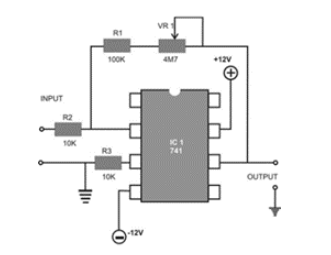
The main applications of the IC 741 include adders, comparators, subtractors, voltage followers, integrators and differentiators. a typical circuit diagram of the IC 741 operational amplifier is shown below. In the circuit below, the IC 741 op-amp is used as a comparator. Even though it is used as a comparator, weak signals are still observed so that they can be identified more simply.
Main applications
There are many electronic circuits currently constructed using IC 741 op-amps, such as voltage followers, analogue-to-digital converters, sample-and-hold circuits, voltage-to-current and current-to-voltage conversions, summing amplifiers, etc. Some of the applications of IC 741 op-amps include the following.
Variable audio oscillators using the IC 741 op-amp.
Adjustable ripple RPS based on the IC 741 op-amp.
Four-channel audio mixing using the IC 741 op-amp.
IC 741 op-amp and LDR-based automatic light control switch.
DC voltage polarity meter using IC 741 op-amps.
Electronic room thermometer using IC 741 op-amps.
Microphone amplifier using IC 741 op-amp.
IC 741 op-amp tester.
Short-circuit based RPS protection.
Thermal contact switch using IC 741 op-amp.
Wind sound generation based on IC 741 op-amps.
Summary
The above is the data sheet about IC 741 operational amplifier, which includes pin configuration, circuit diagram, specifications, application characteristics, etc. I hope it can help you better understand the IC 741 operational amplifier.
As we all know, operational amplifiers are solid-state integrated circuits, which are a fundamental part of analogue electronic circuits and can perform different types of analogue signal processing tasks. These ICs use external feedback to regulate their functions and these components are used as multi-purpose devices in various electronic instruments.