Today more and more switching circuits are being replaced by MOSFETs in triode application circuits. Field effect transistors (FETs) are voltage controlled devices that are simple to drive, fast and have low drive energy consumption and are therefore more widely used in switching circuits. In this paper, some of the triode typical amplification application circuit for more in-depth and analysis and simulation.
1, the basic amplification circuit
Looking back at the school curriculum knowledge, the basic triode circuit revolves around three basic amplification circuits for learning: common emitter amplification circuit, common collector amplification circuit, common base amplification circuit. These three circuits were widely used in the days of discrete transistors, but have now been replaced by the more powerful and stable OPA circuits, or can be found in various analogue ICs.

OPA is easy to use, but to gain a deeper understanding of OPA, it is necessary to “learn from the past”.
Before proceeding with the analysis of the three basic amplification circuits, we need to be clear about one basic rule: the triode is a controlled current source! It is important to note that this controlled current source is bounded (voltage rails)! Based on these two basic guidelines, whatever kind of triode amplification current can be analysed with clarity.
1.1 Common emitter amplification circuit
Figure 1.1 below shows a simplified model of a common emitter circuit, which contains the most basic structure of an amplifier circuit: bias-input-conversion-output. Vbias is the bias voltage, which serves to determine the static operating point of the circuit. Why does an (amplified) circuit need a static operating point? Because the transistor needs to operate in the “linear zone”. Once the transistor is in the linear zone, the circuit problem can be directly converted into a mathematical problem according to the theory of “Circuits”.
The input voltage V1 and the bias voltage Vbias can be obtained using the superposition theorem: Vout = Vout(V1 response component) + Vout(Vbias response component). Where Vbias is the DC component and V1 is the AC component, it is important that we first split the input signal into a DC + AC form.
We talked about the BJT transistor in the previous section: a controlled constant current source model satisfying Ic = β*Ib in the linear operating region.
This time we control Vbias in an intermediate state, i.e. Ib(bias) = (Vbias – 0.7V)/R1 = 1.8mA and Ic(bias) = β*Ib(bias), which is the quiescent operating current of the circuit. The key parameter β of the triode is expressed using DC Gain = hFE, and here it is explained that for low frequency amplification circuits the influence of the parasitic parameters of the triode device itself is not taken into account (infinite bandwidth)! So, for AC analysis the triode’s “AC Gain” = DC Gain = hFE. Generally the triode’s hFE varies between a few tens and a few hundred depending on the application scenario of the tube.
We have already worked out the static operating point according to the circuit principle, so can the AC circuit be solved by the same circuit solving method? Of course you can! But why are we always told in textbooks that “AC equivalent circuits need to be shorted to VCC and GND”? Actually, there is a prerequisite for this: a small signal! What is a small signal, is that we think that the input signal AC amount V1 is small enough to change the operation of the transistor circuit and remain in the “linear operating zone”. Keeping the triode AC circuit in the linear operating zone, Vbias = 0 (i.e. a short circuit), and likewise Vcc is considered to be a DC voltage source, and the response calculation of the direct flow has been completed in the DC bias circuit! Therefore Vcc = 0 (i.e. a short circuit) is also required. Then the small signal AC circuit model shown in Figure 1.2 can be obtained! This completes the analysis and solution process for a typical triode amplifier circuit, and the simulation results are shown in Figure 1.3, where it can be seen that the phase of the output signal and the input signal are opposite.
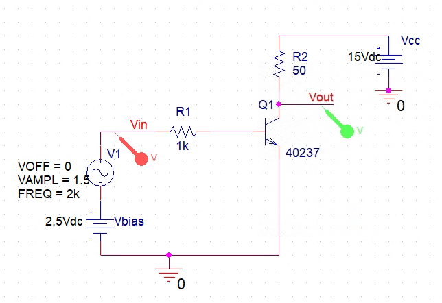
Figure 1.1 Common emitter amplifier circuit
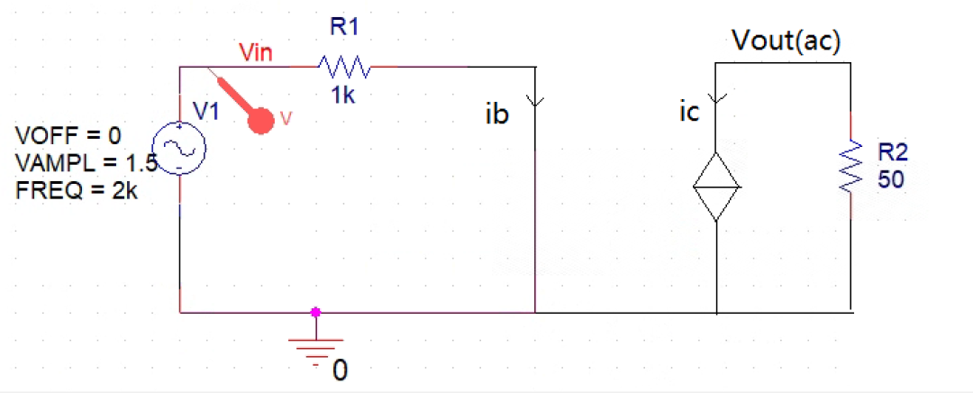
Figure 1.2 Small signal equivalent of the common emitter amplifier circuit
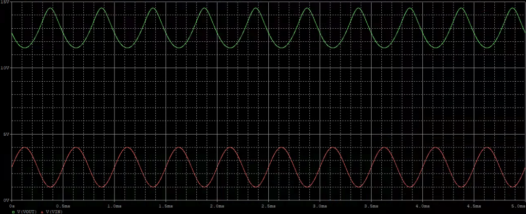
Figure 1.3 Simulated output of the common emitter amplifier circuit
1.2 Common collector amplifier circuit
As shown in Figure 1.4, it is a collector amplifier circuit. Compared with the common emitter circuit this circuit connects the collector directly to Vcc1, then from the small signal equivalent circuit it can be seen that the collector of Q2 will be shorted to GND and become the reference plane, therefore it is a common collector amplifier circuit. It can be seen that as Vin1 increases, the Ic current increases, the Ie current increases, the Vout1 voltage increases, and the output signal Vout1 and the input signal Vin1 are in phase. The simulated waveform of the circuit is shown in Figure 1.5.
From the waveform it can be seen that the input and output are basically the same, there is a certain fixed voltage difference (BE drop of the triode), as the output machine is the emitter of the triode, so the circuit is also called “emitter follower”. Almost no amplification! However, its excellent impedance characteristics can be used in various buffer stage circuits. For large gain transistors the Ib current can be controlled to be very small ≈ 0, so ideally the input impedance is infinite; and the output is led directly from the emitter, with no other lines to divert the voltage, so the output impedance is approximately infinite. This characteristic hardly affects the output signal of the pre-stage, and at the same time has a very strong post-stage carrying capacity!
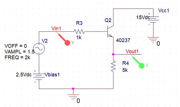
Figure 1.4 Common collector amplifier circuit
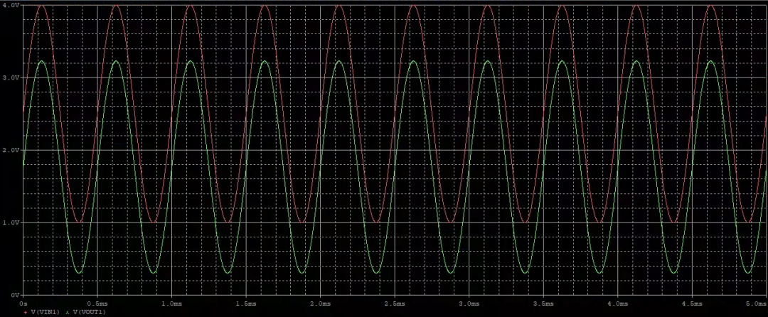
Figure 1.5 Simulated output of the common collector amplifier circuit
1.3 Common base amplifier circuit
A common base amplifier circuit is shown in Figure 1.6. Structurally, Vbias2 provides the DC bias point and the base of Q3 is connected to GND in the small signal circuit, making it a common base amplifier circuit. Looking first at the simulated waveform shown in Figure 1.7, it can be seen that the output waveform is in phase with the input waveform, and since Ic ≈ Ie, the AC amplification is approximately equal to R6/R7 = 5.

Figure 1.6 Common base amplifier circuit

Figure 1.7 Simulated output of the common base amplifier circuit
What is the difference between a common emitter amplifier circuit and a common base amplifier circuit, both of which have the same function of amplifying a signal?
In a practical amplifier circuit, the AC signal needs to be superimposed on the DC bias point and the key to the circuit is the AC coupling. The key to the circuit is AC coupling. The actual circuit cannot be set up with many bias supplies to determine the operating point, as shown in Figure 1.8. “This can cause the circuit to leave the linear operating region, which we do not want. Therefore, it is more common to use the resistive-capacitive coupling form on the right, where Rb determines the DC bias point of the circuit and the AC component of u1 is superimposed by C1, which will not affect the DC bias point of the original circuit and will safely keep the circuit in the ‘linear operating zone’. However, there is a problem here, as C1 and Rb form an RC filter structure, which means that the frequency bandwidth of the circuit cannot be made too high!
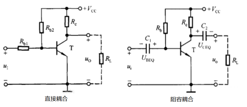
Figure 1.8 Two forms of coupling for the common emitter
Returning to the common base amplifier circuit for analysis, as shown in Figure 1.9
Rb1 and Rb2 form the DC bias voltage of the circuit, Cb is the decoupling capacitor, and the AC impedance of Cb is ≈ 0, shorting out the Rb2 resistor. Since the AC impedance of the emitter is zero, and therefore and the coupling capacitor cannot form an RC filter (R=0), a great increase in bandwidth can be obtained (approximately equal to the bandwidth of the triode itself). However, the input impedance is very small and requires a relatively high driving capability of the pre-stage, while the output impedance is Rc, which is comparable to that of a common emitter amplifier circuit.
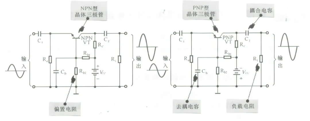
Figure 1.9 AC coupling of a common base amplifier circuit
- Comparison of the application of basic amplification circuits
We compare slightly the three basic amplification circuits, here citing the conclusions in Reference 5.
(1) Co-injected circuits.
The voltage gain and current gain are both higher, the input resistance is in the middle of the three groupings, and the output resistance is strongly related to the collector resistance. Because of these advantages, it is the most commonly used grouping, and it is also possible to cascade multiple common-injection amplifiers to form a multi-stage amplifier for higher gain.
(2) Common-collector circuit.
It only amplifies the current, not the voltage, and has a voltage following effect. Therefore, multiple common-collector circuits cannot be used to form a multi-stage amplifier circuit. However, it has the highest input resistance and the lowest output resistance in the three configurations, and is often used in multi-stage circuits for input and output stages, as well as for intermediate buffer stages.
(3) Common base circuit.
Only amplifies voltage, not current, and has a current-following effect, so it is also not suitable for multi-stage circuits composed solely of common base circuits. The input resistance is small and the output resistance is high,
It can be used as a constant current source. From what we have seen so far, these characteristics do not yet show its outstanding advantages, but in fact the common base amplifier circuit has a very wide passband, which is useful in the field of high frequency and broadband.
A comparison of the parameters of the three basic amplification circuits is shown in Figure 2.1.
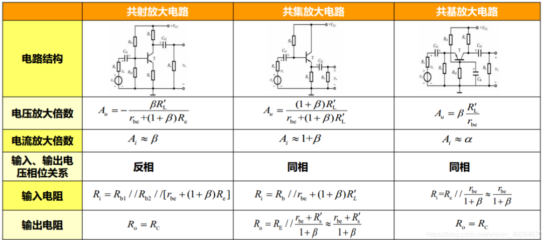
Figure 2.1 Comparison of basic amplification circuits